MOSFET gate resistor

Chris65536

Joined Nov 11, 2019
270
Can I configure the analog input as « disconnected « in between reads ?
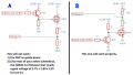
That depends on your microcontroller. I have a very similar circuit, with an ATMEGA328P @ 3.3v reading a thermistor. I turn off the power to the voltage divider between reads mainly to avoid self heating. I also used an N MOSFET, so my A/D input is pulled high most of the time. I never considered there to be any power lost there, so I never bothered to turn off the input. But now I am curious! I can check the voltage drop across the 10K thermistor down to 0.01mV, which would be 1 nA. I'll look into it this evening, and report what I find.
 

Thread Starter

Matt74

Joined Jun 29, 2019
30
great, that’d be interesting.
I should rephrase my question. I know I « can » disconnect the pin, the question is will it change anything regarding possible current flow through it when the MOSFET is OFF.
 

Chris65536

Joined Nov 11, 2019
270
OK, I checked this, and my Fluke meter reads a steady 0.00 mV across the 10K thermistor. So I guess that means it's less than 0.5 nA? Close enough to zero for me!
 

Thread Starter

Matt74

Joined Jun 29, 2019
30
Allright I got so many different information that I start to mix everything up. Which of the following could do, and which one would be the best ?
I am sampling a Force Sensitive Resistor 200us every 20ms. I want to switch the power on only during this time to save battery power. I am using an RF52 controller operating at 2.8V. There are analog and digital power rails (really separated only by a couple of ferrite beads)
Note : LTC1981 is an ultra low power driver but it still uses current. I don't know how it compares to a MOSFET or NPN driver.
Screenshot 2020-01-07 at 10.46.05.png

What would be the pros and cons of each in term of performance ?

Cheers !
 
Last edited:

ci139

Joined Jul 11, 2016
1,992
Only your "B" circuit will work properly.
Yes . . . but it's ON by default . . . another issue is sufficient supply voltage when runned on battery to power the FSR with stable voltage ← also the speed and temperature dependence (drift) of it . . . not to mention the proof (a field test) that it actually will reliably detect anything in practice
. . . it's possible to make the FSR part to be constant ON at microamps -- especially if there's only the 20ms interval
 
Last edited:

Thread Starter

Matt74

Joined Jun 29, 2019
30
Again I ask, how will you connect to the bottom of that tiny little Mosfet?
I know very few people who hand solder SMD components of an entire PCB, so I'll just do like everybody else: I'll let the assembly robot do it for me !

As for the upside down PNP, you're right, it's a mistake. I wanted to make all schematics look alike for better comparison but I forgot about the actual orientation of the components (I only looked at the little numbers)... Sorry. Please ignore the orientation and just consider the layout.

Again I am no EE and it is obvious to everyone at that point that my understanding of MOSFET is... a work in progress... Is there a reliable way to make a high side switch with an N-MOSFET ? Why would't D work (apart from the fact that it is also upside down...)? What about C, is it not the whole point of a driver than to provide enough voltage to the gate ?

LTC1981-4638.png si3442DV is an N-MOSFET used in a high side switch configuration. What did I get wrong ?

Thanks !
 
Last edited:

ericgibbs

Joined Jan 29, 2010
21,444
hi Matt,
Have you actually done a power audit of the full project versus the life expectancy of the battery supply.???
If yes, please post your findings so that we can check the effect of disabling the ADC voltage divider.

E
 

Thread Starter

Matt74

Joined Jun 29, 2019
30
hi Matt,
Have you actually done a power audit of the full project versus the life expectancy of the battery supply.???
If yes, please post your findings so that we can check the effect of disabling the ADC voltage divider.

E
Hi Eric,
Yes I have (based on estimates from a simulator, not actual data) and that is precisely what made me start to think about power saving improvements. It is a battery-powered device and for practical reasons I would like to use nothing bigger than a 20mm coin cell for at least 8h of continuous use. The nRF will draw around 4mA while executing the measurements+calculations and broadcasting then it should drop down to 2-3 uA in sleep mode. The analog part (FSR and divider) would continuously draw 1.87 mA, it is a significant part of the current consumption which can be reduced by 2 orders of magnitude with a switch (well, in theory because the switching components will also use a bit of juice). I looked for ways to do that and I came up with this MOSFET switch thingy which turns out to be way more difficult to implement than I originally thought ! I spent most of my free time last week reading about this stuff and I received a lot of helpful and less helpful advice. I don't fell I made any real progress ... Thanks for taking the time to look into the issue, much appreciated !
 

ericgibbs

Joined Jan 29, 2010
21,444
hi Matt,
Using circuit 'B' as an example, this is what a sim shows.
Depending on the On/Off duty cycle of the Digital control signal, the circuit could be less efficient.
During the Off period the transistor Base requires current in order to keep the MOSFET Off.
I have used high values for Base and Collector resistors.
Look at these plots, see what you think.
E
 

Attachments

Thread Starter

Matt74

Joined Jun 29, 2019
30
Hey Eric, thanks for the sim ! It looks like the duty cycle is 50%. I don't know if you can set your simulator to turn on for 200us instead of 1ms. I don't understand why the peak R1 current is only around 65uA (with R1+R2=11.2K and V1=2.8 it should be 250uA). That means that there is a huge resistance across M1 right ?
Anyway it was kind of my gut feeling that a transistor would be the least efficient method. I was hesitating between C or D but I am more and more tempted to use the low power driver. That seems to be the safest solution for someone who is not 100% comfortable making up his own switch circuitry.
Cheers !
 

Chris65536

Joined Nov 11, 2019
270
3442DV is an N-MOSFET used in a high side switch configuration. What did I get wrong ?
As the N-MOSFET turns on, the voltage at the Source terminal will rise, so Vgs will drop and start to turn itself off. I guess it would end up in the linear region? This is definitely not what you want. You want the full voltage for your load, which leaves no room for Vgs. I think a sinking arrangement would work just fine though. Or a P-MOSFET.

EDIT: Just saw Audioguru's post, which has the answer to this one.
 

ci139

Joined Jul 11, 2016
1,992
R1 is necessary because mosfet gate current is vitally important!
according to data sheet (#19) Pg.156 one can assume 280Ω series output resistance ?? why to add 100 more Ω
it was kind of my gut feeling that a transistor would be the least efficient method
the transistors can operate at nA -s , practically down to about (380...420...)540mV Vcc ← this however restricts (depending on circuit) fast transition times (due https://forum.allaboutcircuits.com/threads/bjt-transistor-storage-time.112878/) --and/or-- lowermost output impedance (Collector resistance)
 

Blakus

Joined Apr 3, 2008
5
Hello, I am designing a MOSFET-based switch to power the analog part of my circuit only when needed in order to save some power and extend the battery life. I am not an EE so I apologise if my questions are a bit naive...

My (rather limited) understanding of MOSFET is that they should not require a gate resistor however I read here SE thread that it could a good idea to prevent ringing. In the same thread they also mention a high impedance resistor to ground. The schematics would therefore look like this (AEN is one of the digital outputs of my microcontroller and A0 is an analog input, there are separate analog and digital power rails):
Q1 Did I pick the right MOSFET ?
I selected a DMN2005LP4K-7 (datasheet) for the following reasons:
  • Rds(on) is very low (400mOhm @2.7V) and my main goal is precisely to save power.
  • The gate threshold voltage is very low (0.5-0.9V) so it should be full on with a logic high of 2.8V.
  • VDD=VDDA=2.8V so with Vds=20V and Vgs=10V I am on the safe side
  • The total resistance (FSR + R3) is so high that I shouldn't have more than 1mA going through so a max drain current of 300mA is plenty and for the same reason 400mW of power dissipation is way more than I will ever need.

Q2 Do I really need R1 and R2 ?
AEN will be forced down by the microcontroller so do I really need the pull down resistor R2? As for R1...

Thanks a lot !
You could also use a transistor for such a load.
 

kbritton

Joined Jan 8, 2017
3
Do you have an unused gpio that you could connect your series resistor and fsr to?
The FSR could be powered by setting the gpio pin high. No need for external mosfet. Depending on the gpio current available.
 

Thread Starter

Matt74

Joined Jun 29, 2019
30
Do you have an unused gpio that you could connect your series resistor and fsr to?
The FSR could be powered by setting the gpio pin high. No need for external mosfet. Depending on the gpio current available.
It crossed my mind but It sounded a bit « dirty ». Is it good practice ? I can’t think of any obvious reason why not after all...
 
Top