Measuring an IC's input resistance

Thread Starter

BlackMelon

Joined Mar 19, 2015
168
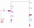
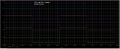
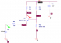
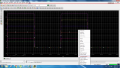
Hi y'all! Thank you for your suggestion, MrChips and Alec_t. I have just figured out how to find the sweeping parameter (Vcc in my case)! Just right click on each trace > Trace Information. The first time I did; I was unable to view the value of Vcc for each particular trace because I did sweeping with too many Vcc values, so the traces are packed too tight.
 

Attachments

Thread Starter

BlackMelon

Joined Mar 19, 2015
168
Alect_t, your circuit works excellently!

In the simulation, the upper waveform is the input of the circuit, the lower one is that of Q2 collector. I sweep the value of Vcc from 0 to 30V (so I got many traces).

What does cause the undershoot in the collector voltage when the input is at the rising edge?
 

Attachments

Alec_t

Joined Sep 17, 2013
14,335
The undershoot is probably due to junction capacitance.
But why are you applying up to 30V? That will fry the IC. The absolute maximum for the HEN input is 16V, but you should use a lower voltage in practice.

Edit:
Here's the circuit with the suggested diode addition.
HEN-drive3.PNG
 

Alec_t

Joined Sep 17, 2013
14,335
Here's the manufacturer's suggested circuit, but modified to make it WORK!
It has the advantage that only one transistor is used and there is no logic inversion.
Have a play with it in your simulator.
HEN-drive4.PNG
 

Thread Starter

BlackMelon

Joined Mar 19, 2015
168
Here's the manufacturer's suggested circuit, but modified to make it WORK!
It has the advantage that only one transistor is used and there is no logic inversion.
Have a play with it in your simulator.
View attachment 130069
Thank you! I'll try it! Thank you for warning me about 30V too. I'm not gonna input that to the Vdd. I just want to see the extreme trend of the circuit. :D

I have a question about driving the IN+ pin of HIP4080A. I took into account the battery (Vcc) drain. The IN- voltage is fixed at Vcc/2. The TTL logic of an MCU is passed to VIN+ via a voltage divider, having 3 resistors. I did a Vcc sweep from 16V down to 7.6V, and saw that the DC level of IN+ is higher than Vcc/2 when Vcc = 7.6V. And, the opposite situation happened when Vcc = 16V.

I was trying to solve this problem, so I made a BJT circuit with 2 base resistors, Rc, and Re. I picked two Vcc values to be 30V and 7.6V (again, I am not going to input 30V to the driver's VDD). I hope that lowering of the battery will lower the Vc bias point. But what I have got is the VIN+ always greater than VIN-.

So, is there any way to address this problem without using switching power supply to fix the Vcc?

EDIT: The voltage divider task is to confine the VIN+ to be in the common mode voltage range of the "IN" comparator.
 

Attachments

Last edited:

Alec_t

Joined Sep 17, 2013
14,335
That voltage divider will cause a greater voltage than the MCU supply to be applied to the MCU pin. The MCU will not be happy!
Why are you applying a TTL output to Vin+? Surely Vin+ is intended as an analogue input (part of an error amplifier)?
 

Thread Starter

BlackMelon

Joined Mar 19, 2015
168
It's gonna be like this. This circuit is suggested by the manufacturer. I under stand that the Vcc will try to pull to Vin+ up high. This sounds strange to me as if the MCU will always sink the output current. The reason they gave me for this circuit is about the ESD protection of pin IN+ and IN-, and the common mode voltage range of the comparator (Vcc-1.5 to 1V).
 

Attachments

Alec_t

Joined Sep 17, 2013
14,335
Ok. So both inputs of the comparator need biasing somewhere in that common-mode range. The bias point should be below the +ve rail of the MCU.
 

Thread Starter

BlackMelon

Joined Mar 19, 2015
168
Ok. So both inputs of the comparator need biasing somewhere in that common-mode range. The bias point should be below the +ve rail of the MCU.
Yes, and thank you for warning me about the voltage greater than MCU. The circuit they gave me has the bias point at IN+ around 2volts, and the voltage swings (peak to peak) of 800mV. So, it will not produce IN+ voltage greater than the MCU output. I raise that bias point up, hoping to address the battery voltage drop problem (to find another problem LOL).

So I'm gonna install a 12V/1.5A voltage regulator for the driver's Vdd. :)
 

Thread Starter

BlackMelon

Joined Mar 19, 2015
168
I am curious about the bias voltage. Here I modified Alec_t circuit by adding 100ohm resistor at the emitter to suppress the sensitivity to the change of R2 (may be because of thermal issue or sth. else).

The 5V-0V pulse was applied like V4 in the file "pulse train", and Vcc was 12V. I viewed V4 as changing of voltage around 2.5V (Vpulse = Vdc + Vac, where Vdc = 2.5V, and Vac is a +2.5/-2.5V square wave). I simulated the Vc bias voltage with the circuit in the file "Bias point". I got Vc around 6V as what I expected.

However, back to the file pulse train, after I applied the Vpulse, the program gave the Vc bias voltage of 647.5mV. Is it supposed to be 6V? What exactly is that value?
 

Attachments

Alec_t

Joined Sep 17, 2013
14,335
If Vdd is 12V then the IN+ and IN- voltages should be somewhere in the allowed range 1V-10.5V.
Here's a mod of my circuit (option 1) which will give a voltage swing from ~1.3V-9.6V, i.e. well within that range, but if you're happy with a more limited swing from ~1.3V-5v then option 2 (essentially what the manufacturer suggested) is a lot simpler.
ComparatorBias.PNG
 
Last edited:

Thread Starter

BlackMelon

Joined Mar 19, 2015
168
You've lost me. HEN is just an on/off signal. Why are you concerned with 'bias'?
Because I want to set the DC offset of the HEN signal to the middle of the Vcc (12/2 = 6V). So, the HEN signal can swing up to +12V and all the way down to about 0V.

I think the HIP4080A is very bizarre. I tried to test the truth table on page 6 of its datasheet. I set up a simple circuit in the attachment. I held DIS pin low to enable the IC, and HEN pin low to disable upper mosfets. According to the truth table, I want to see if I the logic IN+>IN- changes from 0 to 1, the only lower mosfet getting turned on will change from ALO to BLO or not. This was done by holding IN- constant at 3.28Vdc, and tuning the voltage at IN+ by using the voltage divider.
Here is the result:

IN- : Held constant at 3.28Vdc
1) IN+>IN- = 0 (IN+ = +1.2Vdc).............V(BLO) - V(BLS) = 12Vdc, V(ALO) - V(ALS) = 0V
2) IN+>IN- = 1 (IN+ = +4.20Vdc)...........V(BLO) - V(BLS) = 12Vdc, EDIT: V(ALO) - V(ALS) = 0V

According to the page 6 truth table, in the first case, ALO mosfet was supposed to be "ON" ,V(ALO)-V(ALS) = 12V, and BLO mosfet was supposed to be "OFF", V(BLO)-V(BLS) = 0V. And, it should be the other way around for the second case.

Did I violate something?

Thank You
 

Attachments

Last edited:

Alec_t

Joined Sep 17, 2013
14,335
Did you mean to specify the ALO and ALS values for the second case?
I can't see that you've violated anything.
I wonder what the delay circuits do when the FETs aren't being actively switched on/off? Perhaps they produce the effect you're seeing.
 

Thread Starter

BlackMelon

Joined Mar 19, 2015
168
Did you mean to specify the ALO and ALS values for the second case?
I can't see that you've violated anything.
I wonder what the delay circuits do when the FETs aren't being actively switched on/off? Perhaps they produce the effect you're seeing.
I mean that since HEN is held at 0V, IN+>IN- logic adjusted by the potentiometer can yield only two results highlighted in yellow. In one case, the ALO will be turned on, the other is that BLO will be turned on.
What I have got are always-on BLO, and always-off ALO. The IC neglects IN+>IN- logic! T_T
 

Attachments

Top