LTSpice "Time step too small" error

Thread Starter

Hekky

Joined Jun 14, 2015
4
Hello,
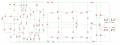
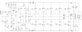
I'm working on an audio power amplifier. I recreated the schematic from the internet in LTSpice and now I'm getting error: "Analysis: Time step too small; time=1e-006;timestep=1.25e-019;trouble with bzx84c15l-instance d1". This is the first time I'm using this program and I have no idea how to fix this.
I also have a second question. I was getting error: "Voltage source V2 and voltage source V3 are paralleled making an over-definied circuit matrix. You will need to correct the circuit or add some series resistance". I added 10Meg, because I read somewhere that the resistance here should be this big. Is this a good solution?
I attach schematics from Eagle, LTSpice and the original one.
 

Attachments

WBahn

Joined Mar 31, 2012
30,088
The "time step too small" error normally comes about because you have something that is trying to change too fast, possibly while trying to solve for the initial operating point for the simulation. I can't tell which device D1 is because you aren't consistent in your reference designations between these schematics and I don't feel like guessing.

You power supplies are not hooked up correctly. The should be between the return side of the speaker and the top/bottom rails. As you have it, you are trying to power your amplifier THROUGH the supply bypass capacitors!
 

WBahn

Joined Mar 31, 2012
30,088
If he corrects the schematic, he won't need any resistor because the two supplies won't be in parallel. If he just changes the resistor to some small value, he will simply have a lot of current in that resistor without having fixed the actual problem.
 

Thread Starter

Hekky

Joined Jun 14, 2015
4
Thanks,
Can you show me how the schematic should look like after correction? The problematic diode is marked as D1 on LTSpice schematic and as D6 on original.
 
Last edited:

WBahn

Joined Mar 31, 2012
30,088
Thanks,
I'll try to correct the LTSpice schematic. The problematic diode is marked as D1 on LTSpice schematic and as D6 on original.
D6 is in the bridge rectifier in the original schematic. Your LTSpice schematic doesn't have the bridge rectifier at all. D1 in your LTSpice schematic is a zener diode over near Q2. Ah, I see that it is also marked D6. That schematic has two D5 and two D6 designated parts.

Correct the power supply problem and see if that makes the time-step problem go away. If not, we can deal with it then.
 

Thread Starter

Hekky

Joined Jun 14, 2015
4
Correct the power supply problem and see if that makes the time-step problem go away. If not, we can deal with it then.
Can you show me how exactly can I correct this? I'm not sure if I understand the solution.
 

WBahn

Joined Mar 31, 2012
30,088
How, exactly, is CON2 supposed to be wired up to the rest of the world? I'm particularly interested in how the center pin is related to the AC power that is provided on the other two pins.
 

ronv

Joined Nov 12, 2008
3,770
Yes, the supply I think. Try grounding the right side of R37 in the spice schematic. It might help if you posted the .asc file.
 

ebeowulf17

Joined Aug 12, 2014
3,307
For starters, I agree with Alec's recommendation above.

Also, I got the exact same error about a week ago and simply adding a ground through a high-value resistor (500M) to my isolated high voltage side solved the problem. Here are a couple links that might explain better than I can:

http://microcontrollers.2385.n7.nabble.com/LTSpice-grounds-problem-td44955.html

http://www.electronicspoint.com/thr...-with-floating-nodes-on-using-relaysw.123096/

Olaf,
I didn't look at your circuit, but the guideline is that EVERY node
needs to have a DC path to ground. Some parts, like transformers and
transmission lines modeled via 'behavioral' modeling, don't have a
path through them for DC, so you have to have an actual ground at both
ends.

You mentioned having different grounds for different areas of the
circuit. To do this, you use a 'buffered' ground, a ground isolated
by a large resistance, such as 10MEG, or even 1G between the ground
and the circuit in question. You still have the DC path so that the
simulator can establish voltage levels, but the 'ground' level between
the two sections can now be at different levels.

For more info, look at:
http://edmondsonengineering.com/grounds.aspx


Charlie

Dec 17, 2008
 

Thread Starter

Hekky

Joined Jun 14, 2015
4
Thank you, I changed my schematic to this and now there are no errors.
But, in the original schematic there were BD911/912, BC550, 2SK1530/2SJ201 transistors and 1N4007 diode - I'm not sure which elements in LTSpice can substitute them. I attach my .asc model.
There was supposed to be 300W on the load (8ohm) with 1.5V input voltage (according to the datasheet of this schematic).
 

Attachments

Top