Looking for help choosing a transistor

SgtWookie

Joined Jul 17, 2007
22,230
Sgt,
if the application is for normally on and short durations of LED off, it should be little issue.
Actually, there ARE some issues.

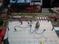
Our OP stated that they are using LEDs rated for 12v operation. I'm assuming that they have intrinsic current regulation or embedded resistors.

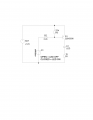
In order to implement your suggestion, they would have to add another resistor in series with their ready-to-run 12v LED. If it had intrinsic current regulation, that could work out just fine. If it had an embedded resistor, it would be much less bright than if it were operating on it's own.

When you shunt around the LED, the current through the limiting resistor will increase a great deal, because you've removed the Vf of the LED from the loop. The resistor would need to be rated for the additional power dissipation so as to not burn up.
 

VoodooMojo

Joined Nov 28, 2009
505
maybe I will start reading the whole thread!

Sgt,
after reviewing this entire thread, i will admit that i missed a bit of the info.
I was eager to point out that the desired outcome could be obtained in the enhancement mode but efficiency was not my target.
sometimes what does work will work better another way.

thanks for yet another voodoo pin-stick to the forehead.
 
Last edited:

Thread Starter

gte

Joined Sep 18, 2009
363
Sgt, if I understood your post, I can do the following and it would work just fine?

Just to make sure I do understand the circuit, it appears that 2n2222 transistor is an NPN type and with this circuit, even though the transistor is normally open by itself, it is basically normally closed here because it is always receiving +12v to the base, which is much higher than the ground (<--is that the correct terminology, or maybe 0v?) that it's receiving at the collector and passing to the emitter.

Then when the switch is closed, it creates a short circuit for the 4.7k resistor (which is a pull-up resistor?) and then it gives 0v the base pin and it breaks connection between the collector and emitter?

Is this correct?


The original circuit was posted as an example, I have a circuit a little more complicated that I'd like to try this with as well.


Ugh - shorting around the LED is a tremendous waste of power.

Believe it or not, that's one of the first mistakes I made on this site.

Here's a way you could do it with either an enhanced-mode N-channel MOSFET or an NPN transistor:


When a switch is closed, the corresponding MOSFET or transistor is turned off; otherwise the 4.7k resistor connected to the gate or base turns the device on. The bad part about this design is that to turn the LED off, there will always be 2.5mA current flowing through whichever 4.7k resistor. However this is much less costly than shunting the current around the LED.

Rledn is assumed to be part of the LED.

I don't know why you ordered MOSFETs with such a high Vdss rating. If you're working with 12v automotive stuff, 55v is about as high as you'd need unless you were working on the ignition system.

There are several items that are important to learn about enhanced-mode power MOSFETs. While MOSFETs can be very efficient, making a poor choice can lead to very poor circuit performance.

Vdss rating - generally, you want to choose one that's about 1.5 times the expected circuit voltage.
Id and Rds(on) rating - high for ID, low for Rds(on).
Gate Charge (nC) - lower is better for switching times.
Unfortunately, these are all in conflict with each other. :(

If you want a low gate charge, you'll need to find the best trade-off between Vdss, Id and Rds(on) that you can.

If you go for high voltage ratings, expect a higher Rds(on) and lower Id. You can bring the Rds(on) and increase the Id by increasing the gate charge.

Logic level or standard level are related. Logic level MOSFETs (almost all of them N-channel) are very handy for driving directly from uC's (microcontrollers). Over the last decade, there have been boatloads of new MOSFETs introduced in the logic level category. If a MOSFET is not specifically rated for logic level (4.5v-5v), your circuit performance will vary when trying to use logic-level voltages on the gate. Standard level MOSFETs are those which are not specifically rated at a logic level. Their specifications are given with Vgs (voltage at the gate with respect to the source) equal to 10v.

A really easy-to-use logic level MOSFET is an IRLD014. It can sink up to 1.7A, and it's in a 4-pin DIP package which works great on breadboards and prototype boards. There is also the 2N7000, which comes in a TO-92 package - which while not specifically rated for logic level, frequently works OK for low power applications.
 

Thread Starter

gte

Joined Sep 18, 2009
363
Will it also work in this circuit?

I'm guessing no, because the values going to the base and to the collector are both grounds, so the base can't be .7v higher lower than the collector?


nomurphy

Joined Aug 8, 2005
567
The original circuit was posted as an example, I have a circuit a little more complicated that I'd like to try this with as well.


http://img204.imageshack.us/img204/3...tor2n22221.jpg

The circuit you show above will work the opposite of what you indicated in your initial post -- the LED will be OFF when the switch is closed.

The circuit that I proposed in the PDF file using a PNP will work as you first indicated. Note the xstr is a 2N3906 and is very common (other general purpose PNP's will work as well), it's NPN compliment is the 2N3904.

Yes, the 22K is a pull-up that holds the xstr off when the switch is open.
 
Last edited:

SgtWookie

Joined Jul 17, 2007
22,230
Just so you know, you have reversed the labeling of the emitter and the collector.

The emitter of a BJT (npn or pnp bipolar junction transistor) is the leg with the arrow. With an NPN transistor, the arrow is pointing away from the base. With a PNP transistor, the arrow is pointing towards the base.

Since you know that the emitter has the arrow, and that the arrow is pointing either at or away from the base, two of the three leads are known; the collector is the remaining lead. In this case, the collector is on top, emitter on the bottom.

Sgt, if I understood your post, I can do the following and it would work just fine?

Just to make sure I do understand the circuit, it appears that 2n2222 transistor is an NPN type and with this circuit, even though the transistor is normally open by itself, it is basically normally closed here because it is always receiving +12v to the base, which is much higher than the ground (<--is that the correct terminology, or maybe 0v?) that it's receiving at the collector and passing to the emitter.
A BJT is a current-controlled device. A MOSFET is a voltage-controlled device.

What you're dealing in this circuit is a bjt, or current controlled device. The 4.7k Ohm resistor sources current to the base of the NPN transistor. At low current, the Vbe (voltage on the base in respect to the emitter) will be around 0.7v (just for convenience' sake). So, since I = E/R, Ib = (12v-0.7v) / 4.7k = 11.3/4700 = 2.4mA (rounded off).

In order to guarantee saturation, the basic rule is:
Ib=Ic/10 - or in other words, take your desired collector current, divide that by 10, and use that for your base current. Increasing the base current will not increase the collector current any further.

In this case I've made a wild guess and estimated that your LED will require less than 25mA. So, 25/10 = 2.5mA. In this case, 2.4mA is close enough.

Then when the switch is closed, it creates a short circuit for the 4.7k resistor (which is a pull-up resistor?) and then it gives 0v the base pin and it breaks connection between the collector and emitter?
That's pretty much it; the current source to the base is removed. Since there is no current flowing into the base, the collector current falls to nearly zero.

The original circuit was posted as an example, I have a circuit a little more complicated that I'd like to try this with as well.


OK.

When you're editing these photos, you should use .png format. .jpg is a lossy format; the more you edit them, the more fuzzy they'll get.
 

SgtWookie

Joined Jul 17, 2007
22,230
Will it also work in this circuit?

I'm guessing no, because the values going to the base and to the collector are both grounds, so the base can't be .7v higher lower than the collector?

If the switch is open, the base will be kept pulled to ground, so the transistor will not conduct.

If the switch closes, there will be an unlimited amount of current flowing through the base of the transistor to the emitter, and the transistor will heat up and explode with a loud "bang" as it's guts boil. :eek:

BJT's require that you limit their base current and Vbe (base emitter voltage). If you do not, then they will quickly get burned up.

Just as few quick notes....
2N2222 transistors are rated for 800mA absolute maximum Ic. However, their useful Ic is about 1/2 that; around 500mA.
Since 500mA is the realistic maximum, there is no reason to provide the base with more than 500mA/10=50mA current.

You'll find that most transistors will have a useful maximum Ic of about 1/2 their rated absolute maximum Ic.
 

Thread Starter

gte

Joined Sep 18, 2009
363
Just so you know, you have reversed the labeling of the emitter and the collector.

The emitter of a BJT (npn or pnp bipolar junction transistor) is the leg with the arrow. With an NPN transistor, the arrow is pointing away from the base. With a PNP transistor, the arrow is pointing towards the base.

Since you know that the emitter has the arrow, and that the arrow is pointing either at or away from the base, two of the three leads are known; the collector is the remaining lead. In this case, the collector is on top, emitter on the bottom.


A BJT is a current-controlled device. A MOSFET is a voltage-controlled device.

Sgt,

Since the arrow points away, why are the collector and emitter oriented that way? The electrons are flowing against the direction of the arrow in the diagram you posted, correct? If so, that is what confused me. I appreciate the info about how to read the NPN and PNP transistors symbols, I did not know that. Let me ask, can the current flow either way and it not matter? From the collector to the emitter, or from the emitter to the collector?

Also, thanks for the comparison from the bipolar to the field effect, awesome information!


Does this diagram look correct?


What you're dealing in this circuit is a bjt, or current controlled device. The 4.7k Ohm resistor sources current to the base of the NPN transistor. At low current, the Vbe (voltage on the base in respect to the emitter) will be around 0.7v (just for convenience' sake). So, since I = E/R, Ib = (12v-0.7v) / 4.7k = 11.3/4700 = 2.4mA (rounded off).
Why is voltage at the base only .7v?


In order to guarantee saturation, the basic rule is:
Ib=Ic/10 - or in other words, take your desired collector current, divide that by 10, and use that for your base current. Increasing the base current will not increase the collector current any further.

In this case I've made a wild guess and estimated that your LED will require less than 25mA. So, 25/10 = 2.5mA. In this case, 2.4mA is close enough.
Everything makes sense except for you saying that "increasing the base current will not increase the collector current any further" ... unless the collector current is limited/capped by the LED?


That's pretty much it; the current source to the base is removed. Since there is no current flowing into the base, the collector current falls to nearly zero.


OK.

When you're editing these photos, you should use .png format. .jpg is a lossy format; the more you edit them, the more fuzzy they'll get.
Ah ha! I thought the voltage dropped to 0, but it's the current that drops to 0, because it has a path of easier travel straight to ground through the switch? I calculated the resistor would have to be at least 28 ohms to limit current to 500mA? Is my math correct? And the circuit should look like below?


Thread Starter

gte

Joined Sep 18, 2009
363
Hi Nomurphy,

I had 2 circuits I wanted to build, the first with an LED, and the second as an input to an ECU in my car. I was trying to figure out a circuit that works as an inverse to the original circuit you posted, as my second circuit works inverse to my first LED circuit.

Do you think this circuit will work best, or do you propose something else?


The circuit you show above will work the opposite of what you indicated in your initial post -- the LED will be OFF when the switch is closed.

The circuit that I proposed in the PDF file using a PNP will work as you first indicated. Note the xstr is a 2N3906 and is very common (other general purpose PNP's will work as well), it's NPN compliment is the 2N3904.

Yes, the 22K is a pull-up that holds the xstr off when the switch is open.
 

SgtWookie

Joined Jul 17, 2007
22,230
Sgt,

Since the arrow points away, why are the collector and emitter oriented that way? The electrons are flowing against the direction of the arrow in the diagram you posted, correct? If so, that is what confused me.
That's because there are two different ways to look at the flow of current.
Conventional current flow (ie: the current flows from positive to negative; "hole flow")

Electron flow (the flow of electrons from the more negative potential to the more positive potential)

In conventional flow theory, the current goes in the direction of the arrows.
In electron flow theory, the current goes against the direction of the arrows.

That's why it's confusing.

I appreciate the info about how to read the NPN and PNP transistors symbols, I did not know that. Let me ask, can the current flow either way and it not matter? From the collector to the emitter, or from the emitter to the collector?
That normally doesn't happen when you're using them as a saturated switch. The emitter is connected either to Vcc (PNP) or GND/Vee (NPN), so the emitter is at the highest or lowest potential in the circuit.

Also, thanks for the comparison from the bipolar to the field effect, awesome information!
Keep in mind that my example circuits were regarding enhanced-mode FETs only, not depletion-mode FETs.

Does this diagram look correct?

You have the drain and source labels reversed.

Why is voltage at the base only .7v?
If you ignore the collector completely, the base-emitter junction is (electrically) a forward-biased PN junction, or a diode. The Vf of the base-emitter junction will vary with the current through the junction. As the current flow becomes higher, the Vf will also become higher, and since P=EI, the power dissipation will eventually exceed the power rating of the device package.


Everything makes sense except for you saying that "increasing the base current will not increase the collector current any further" ... unless the collector current is limited/capped by the LED?
When a transistor is well-saturated, any further increase in base current will not make a noticeable increase in collector current. The Vce will be quite low.

If your 12v-rated LED will only pass 25mA, it wouldn't make sense to allow more than 2.5mA base current; as you would not realize any more current flow through the LED.

Ah ha! I thought the voltage dropped to 0, but it's the current that drops to 0, because it has a path of easier travel straight to ground through the switch? I calculated the resistor would have to be at least 28 ohms to limit current to 500mA? Is my math correct? And the circuit should look like below?
Rb=(V-Vbe)/(Ic/10)
You're using 8v for V
Ic max is 500mA
With that much current, Vbe will be around 1v.
So,
Rb=(8-1)/(500mA/10)
Rb=7/50mA
Rb=140 Ohms.

28 Ohms would be far too low.

[/QUOTE]
 

VoodooMojo

Joined Nov 28, 2009
505

GTE,

This is the circuit nomurphy sent I think, except for the mislabeling of the emitter-collector.

photos of the circuit breadboarded are attached.

with the switch off-LED on you will see there is 1.53 ma in the base-resistor circuit.
with the switch on-LED off you will see there is 2.63ma in the resistor-switch circuit
 

Attachments

nomurphy

Joined Aug 8, 2005
567
No, the circuit I proposed uses a PNP, not an NPN, in order to comply with the OP's initial requirements. (And, the PNP xstr is drawn correctly.)
 

Attachments

VoodooMojo

Joined Nov 28, 2009
505
No, the circuit I proposed uses a PNP, not an NPN, in order to comply with the OP's initial requirements. (And, the PNP xstr is drawn correctly.)
wow!
this is a confusing mess (to me).

the schematic I posted and attributed to you ( i am sorry for doing that) has a 2222 npn in it.
It looks like part of the one that Sgt sent him.


I will refrain from butting in and out of these threads.

ta ta!
 

Thread Starter

gte

Joined Sep 18, 2009
363
The "butting in" is quite alright, no worries :)


Will this circuit work as I've altered it?


Last edited:

SgtWookie

Joined Jul 17, 2007
22,230
It'll work.

If it's a red LED, you'll get about 10mA current through R1, and about 4.3mA current through R2, for about 14.3mA current through the LED.
 

Thread Starter

gte

Joined Sep 18, 2009
363
Sgt,

Can you tell me how you calculated that?

Did you use I=E/R ? Does the estimated current allowed by the LED come into play with this?


It'll work.

If it's a red LED, you'll get about 10mA current through R1, and about 4.3mA current through R2, for about 14.3mA current through the LED.
 

SgtWookie

Joined Jul 17, 2007
22,230
Sgt,

Can you tell me how you calculated that?

Did you use I=E/R ? Does the estimated current allowed by the LED come into play with this?
I cheated; I simulated it ;)

But yes, it can be done using Ohm's Law and some assumptions.

Assuming the Vf of the LED would be about 1.8v, the BE junction would be around 0.7v:
12v-(1.8+0.7)=12-2.5 = 9.5; 9.5v/2.2k Ohms = 4.32mA base current.

Then, figure the transistor is pretty well saturated, so Vbe will be very low - maybe 100mV or less. Anyway, we'll thrown it in there.
12v-(1.8+.1)=12-1.9 = 10.1; 10.1v/1k Ohms = 10.1mA.
So, 4.32mA + 10.1mA equals...
14.42mA.
 
Last edited:

SgtWookie

Joined Jul 17, 2007
22,230
On bjt orientation:
Have the arrow in the emitter pointing towards the bottom portion of the schematic.
For a PNP transistor, the emitter arrow points towards the base; so in order for the arrow to point down, the emitter needs to be on top.
For an NPN transistor, the emitter arrow points away from the base, so the emitter goes down.

Whenever possible, orient the base towards the left side of the schematic.

When drawing schematics, you should always try to keep the more positive voltages towards the top, more negative voltages towards the bottom.
Inputs come from the left, outputs go towards the right.

This makes it easier to understand the schematic, as most are drawn that way.
 
Top