Facebook
 Google
 GitHub
 Linkedin
Hello Eric,@ericgibbs
Hello again Eric
Great job thank you very much !
It raises some questions and unfortunately the webmaster informed me that until I reach 10 post I can't send a private message.
Could we contatct on Linkedin?
Here are my questions :
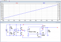
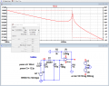
1 -I think you are using a software like LT spice, which one is it ?
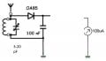
2 - Could you explain me what are the roles of C3, C4 and C5 ?
3- On the left of R3, there is an arrow. Where should it be connected to ?
4- The 2 circuits are connected together or is it on the left just an example to get a VG (Virtual Ground ?) ?
Thank you !
Philippe