Hello,
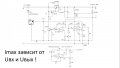
I have a few questions about the attached schematic of power supply.
1. Is the schematic functional ? If not, what are the mistakes in the schematic ?
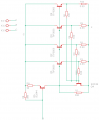
2. Is the layout correct ? If not, how it can be improved ? The DRC does not return any error, but I am wondering about ground connection and other stuff like this...
3. Is the minimum output current really 0A ?
4. I will use R3=680R, R4=2K2, R7=12K, R11=120K, because I did not found the specified values at the local electronics shop. On the VT4 footprint I will solder the wires that go to the power transistors that will be on another PCB.
Here you can find the schematic image: https://imgur.com/NqGeRTi
I have a few questions about the attached schematic of power supply.
1. Is the schematic functional ? If not, what are the mistakes in the schematic ?
2. Is the layout correct ? If not, how it can be improved ? The DRC does not return any error, but I am wondering about ground connection and other stuff like this...
3. Is the minimum output current really 0A ?
4. I will use R3=680R, R4=2K2, R7=12K, R11=120K, because I did not found the specified values at the local electronics shop. On the VT4 footprint I will solder the wires that go to the power transistors that will be on another PCB.
Here you can find the schematic image: https://imgur.com/NqGeRTi
Attachments
-
19 KB Views: 106
-
 94.6 KB Views: 43
Last edited: