LF398 cap charging when hold when power mosfet commutating

Thread Starter

Fernando_1562838485

Joined Jul 11, 2019
8
Hello,

I am working on a project with a boost converter where i need a sample and hold to keep the power value for a short period of time (10 - 50 ms). I have the circuit mounted on a PCB and the S&H works fine until it starts commutate the MOSFET.

here is lf398 datasheet http://www.ti.com/lit/ds/symlink/lf198-n.pdf
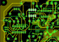
upload_2019-7-11_12-28-19.png
my schematic
upload_2019-7-11_12-27-34.pngupload_2019-7-11_12-42-25.png

In this image u can see that S&H works fine
upload_2019-7-11_12-8-53.png

and if i manually modify the power with and external power resistor it also works as u will see in next image

upload_2019-7-11_12-13-28.png
So when my MOSFET starts to commutate while the sample period is on the S&H outputs the same than input (OK) but when is holding time the capacitator starts to charge up to Vcc voltage.
upload_2019-7-11_12-18-19.png
Here Blue is S&H output and red intput in detail to see what really happens. Next one is what happens when it starts to commutate
upload_2019-7-11_12-20-2.png

Thins that i tried:
  • mounted the same S&H circuit with all caps that says on datasheet on and external protoboard and it did the same thing.
  • make commutate the mosftet with an external function generator
  • try the same two first point with another LF398 IC
I would be very thankfull if anyone can help me and figure out what is going on with this S&H
 

Alec_t

Joined Sep 17, 2013
14,280
The input pin of the LF398 is very suceptible to interference.
Does your pcb have the guard ring arrangement, as per Fig 24 of the datasheet, and the recommended analogue/digital trace separations?
Is the offset-adjust pin floating?
 

Thread Starter

Fernando_1562838485

Joined Jul 11, 2019
8
The input pin of the LF398 is very suceptible to interference.
Does your pcb have the guard ring arrangement, as per Fig 24 of the datasheet, and the recommended analogue/digital trace separations?
Is the offset-adjust pin floating?
Thanks for your thoughs

Yes, the offset-adjust pin si floating, if i check voltatge is Vcc. I tried adding the offset circuit and does the same thing.

I don't have any guard ring but as you can see in following images logic line is pretty far from either input and Ch :
upload_2019-7-12_18-27-19.png
upload_2019-7-12_18-27-13.png
magenta is GND, red is +Vcc and blue -Vcc
I tried without the others IC connected and does the same thing.
This is my clock circuit:
upload_2019-7-12_18-28-48.png
upload_2019-7-12_18-34-19.png
green is sclock (sample logic input), magenta clock, blue V_Cs and Red V_R30

I'll try lower the high logic level down to 2.5 V as datasheet says will help
 

Attachments

Alec_t

Joined Sep 17, 2013
14,280
You have the +15V power rail running right next to and parallel to your signal input (potencia). Any noise on the power rail could easily get coupled to the input signal line :(.
 
Last edited:

Thread Starter

Fernando_1562838485

Joined Jul 11, 2019
8
You have the +15V power rail running next to and parallel to your signal input (potencia). Any noise on the power rail could easily get coupled to the input signal line :(.
Also, you see both intputs and outputs of S&H and input doesn't seem to have any interference i mean the input value is correct
Blue output, red input

and with constant input and more detail of what really happens
 

Thread Starter

Fernando_1562838485

Joined Jul 11, 2019
8
I got it fixed, before LF398 input and output where drived into a LM393 comparador. Adding a buffer amplifier ua741 at LF398 output fixed.
I also incresead sample capacitator from 10 nF to 100 nF.

Thank you for your support though
 
Top