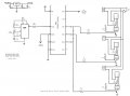
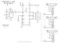
That's a lot of work to watch 10 LEDs light up in one and a half seconds...This all happens in approx 1500ms.
I hope I'm not replying to a closed thread, but here goes anyway:It's a matter of balancing how much current the 4000 series CMOS IC's can source or sink, keeping in mind the current it takes to light the LEDs, along with what voltage is required to operate the logic portion of the circuit.
Even 2.2k Ohms was pushing it. With Vdd=12v, sourcing 4mA will cause the IC's output to drop a volt or two according to the datasheet.
Is that because of the inability of the 4017 to sink the current? How do you figure the total load on the 4017, just add up the current usage downstream? If that's so, then my problem is understanding how to account for the voltage drop you mentioned across the 4017 in the current equation for the MOC's.Well, you're still going to run into problems; you copied Oxbo's earlier schematic. By the time OUT3 is trying to keep all of the transistors turned on, it's probably not going to work very well - if at all. I'd forgotten about that part.
It has very limited source OR sink current ability. It's one thing if you're just driving a single LED or single series string of LEDs from the output; but if you're trying to source current to parallel strings - forget it. You need about 11mA-12mA through each MOC3011's emitter, and there is no way that a single 4017 output can source that much current. I don't think it'll even work for the total 6mA required by the new circuit I posted.Is that because of the inability of the 4017 to sink the current?
Basically, but it's more complicated than that. You also have the Vf of the diodes in the circuit to contend with. Using an AND or and OR gate as a buffer in each stage will help to keep the voltage/curret up, as each will only be driving one load plus the downstream logic.How do you figure the total load on the 4017, just add up the current usage downstream?
Each MOC needs 11mA-12mA to fire the emitter. That's why I changed it from a current source configuration, to a current sink using NPN transistors. The 4017 can source a couple of mA, but not 11-12mA for multiple LEDs.If that's so, then my problem is understanding how to account for the voltage drop you mentioned across the 4017 in the current equation for the MOC's.
Kind of overkill for this. What you need now is an AND or an OR gate to keep the current/voltage up.Would one of the LED driver chips that you mentioned earlier (msg#47 - ULN2004) make more sense here?
That's far too much current for the LED or the 4017 to handle. The MOCs have a max recommended 16mA current through the emitter. The emitter has a typical Vf of 1.15v. I added on another 100mV for the Vce of the transistor when saturated, for a total of 1.25v.I will note that it does work as I have it breadboarded now, but am concerned about that small 22 ohm resistor on OUT1 passing too much current to the MOC3011 (50mA max limit, I think). This based on your earlier warning to Oxbo on driving the LED's too hard.
5v should be OK, but you're going to need another AND or OR gate to cascade the signal.And I'd rather use the 7805 (5V) regulator the schematic reflects instead of the 7812 (12V) I have plugged into the breadboard now.
OK, good.Thanks for the safety advise, I'm not sure how it's wired up now (hot vs. neutral - I'm 150 miles from the project and can't check until Thursday), but I do at least have it fused (on each line), though it's not shown in the schematic. And I am using Q4015 triacs to carry the load, so the triac part of the MOC's should be OK.
Yes. The Neutral line is grounded at the breaker panel. Even under moderate loads, the Neutral line should be less than a couple volts away from ground. However, it is not a replacement for an actual ground wire. Whenever possible, use the actual ground as a chassis ground to protect the humans using the device. Neutral and ground should never be connected after leaving the breaker panel.Dumb question follows - why is neutral safer than hot on an AC line (because neutral is wired to ground in the breaker panel)?
As previously noted, I'm not home so I can not build this circuit, but knowing that I have some CD4073BE triple input AND gates, does this circuit look viable? Based on the 4073 datasheet that this chip can handle 500mW, I figured I could dump the transistors and drive the MOC's directly. Am I right?5v should be OK, but you're going to need another AND or OR gate to cascade the signal.
Nope, sorry - not running from 5v.As previously noted, I'm not home so I can not build this circuit, but knowing that I have some CD4073BE triple input AND gates, does this circuit look viable? Based on the 4073 datasheet that this chip can handle 500mW, I figured I could dump the transistors and drive the MOC's directly. Am I right?
Not from 4000-series CMOS outputs when Vdd=5v.I also assumed the output from the AND gate to be 5V, so I have a calculation of 5V-1.15V/0.0115 which puts me right around a 330 Ω resistor. Is that correct too?
Neutral and Line, respectively.What do the N and L notations stand for on the AC line?
I've been at it a couple weeks longer than you haveI appreciate your help here, you obviously know far more than me about all this stuff. Thanks.
I'm looking at the datasheet, but I'm not really sure that I can discern the data that shows the voltage drop. Looking at the textual "Characteristics" section it shows the output voltage (VOH) as 4.95-5.0 on a 5V input. Now VIH shows 3.5 to 2.25 volts - does this signify the voltage loss?Download Motorola/ONsemi's datasheet for the MC14001B Series. You'll see that when Vdd is 5v, the output voltage drops like a rock at even light loads.
Nope - that's shown in the plots.I'm looking at the datasheet, but I'm not really sure that I can discern the data that shows the voltage drop. Looking at the textual "Characteristics" section it shows the output voltage (VOH) as 4.95-5.0 on a 5V input. Now VIH shows 3.5 to 2.25 volts - does this signify the voltage loss?
Negative numbers are when current is being sourced from rather than sunk to the device.The graphs are another area I don't quite grasp - are they too showing voltage loss? And what's with the negative numbers in the current axes?
Sounds good - have funI'll breadboard the schematic you've modified when I get home on Thursday and let you know how it works out. Thanks again.
Chuck
Thank you for that. I can definitely see how quickly the power loss adds up now. Wow, that's steep!Nope - that's shown in the plots.
Negative numbers are when current is being sourced from rather than sunk to the device.
Here's the plot I was talking about:
See how it's for 5v power? I've marked the spot where the current source is for the 3.9k resistors; about -1mA. You'll lose about 0.5v from Vdd, and measure about 4.5v on the output pin. This is enough for the next stage to "see" a logical "1" as an input.
Thread starter | Similar threads | Forum | Replies | Date |
---|---|---|---|---|
R | timed sequencing switch circuit design | Digital Design | 40 | |
N | Push on push off momentary to activate sequencing relay for a volvo OD | General Electronics Chat | 11 | |
TTL Frequency counter: Sequencing latch/reset | Test & Measurement | 6 | ||
C | Sequencing LEDs | General Electronics Chat | 13 | |
H | Power Sequencing | Power Electronics | 4 |
by Duane Benson
by Jake Hertz
by Duane Benson
by Jake Hertz