Layout of differential pair and impedance matching

MrAl

Joined Jun 17, 2014
13,765
can I check your talking about the diff pairs that cross at 90 degrees to each other ?

standard board, thats 1.6mm thick, in a 100 ohm differential pair ,
are we looking at micro strip or strip line now ?
What do you mean about the 90 degrees, what do you want to know?

You mean a standard 2 sided board where you have one ground plane and one signal trace?

For strip line don't you need a multi layer board?

I'm not an expert on this so you should read up a lot on each type.
The 90 degrees is just about keeping signals apart and that's easy to understand.
The micro strip vs strip line I would think would also be about radiation effects and external noise.
 

drjohsmith

Joined Dec 13, 2021
1,630
What do you mean about the 90 degrees, what do you want to know?

You mean a standard 2 sided board where you have one ground plane and one signal trace?

For strip line don't you need a multi layer board?

I'm not an expert on this so you should read up a lot on each type.
The 90 degrees is just about keeping signals apart and that's easy to understand.
The micro strip vs strip line I would think would also be about radiation effects and external noise.
sorry, I was just trying to understand what actual system / picture your calculation was revering to .

its common at Ghz frequencies to use pair over a plane , thus coupling between pairs on top / bottom is next to zero .
 

MrAl

Joined Jun 17, 2014
13,765
sorry, I was just trying to understand what actual system / picture your calculation was revering to .

its common at Ghz frequencies to use pair over a plane , thus coupling between pairs on top / bottom is next to zero .
Oh that was for just two sides, with traces running on both sides and crossing at a 90 degree angle.
 

drjohsmith

Joined Dec 13, 2021
1,630
Oh that was for just two sides, with traces running on both sides and crossing at a 90 degree angle.
Differential traces crossing at 90 degrees on each side of the board, where the thickness of the board is much larger than the pair gap is going to be insignificant ..
But at these frequencies , the op is going to have to be using a ground plane anyway
 

Rf300

Joined Apr 18, 2025
112
With MIPI-DSI we are talking about clock frequencies of some 100 MHz and signal rise and fall times of about 100 ps. This means we are working with frequencies in the GHz range. For those signals it is absolutely important to follow high speed layout guidelines and to have a proper ground plane.So you need at least a 4-layer board. A simple dual layer board where you fill the area between your signals is simply garbage (sorry to tell that). You will get discontinuities of the characteristic impedance of your transmission lines which will cause signal reflections and disturbance. You also need a length matching between the individual signal pairs because otherwise you will get different propagaion dely for your signals.

As a first starting point you should read this TI Appnote.
 

MrAl

Joined Jun 17, 2014
13,765
Differential traces crossing at 90 degrees on each side of the board, where the thickness of the board is much larger than the pair gap is going to be insignificant ..
But at these frequencies , the op is going to have to be using a ground plane anyway
Hi there,

What do you mean by the "pair gap", the pair gap is the board thickness :)

Imagine looking down at the two-layer board at two traces crossing at 90 degrees to each other. You'd see a plus sign type joint "+" where the horizontal line in the plus sign is the top of the board trace, and the horizontal line in the plus sign is the trace on the underside of the board.

The inductive coupling is theoretically zero, but the capacitive coupling is nonzero because of the tiny square the two traces make as one is immediately over the top of the other. The coupling starts as the area the two traces create with one above and one below (two plates of a capacitor) but there is some additional coupling due to the fringing field that can bring in as much as 40 percent more capacitance. It is very low though as you can see from the formula I posted, but as frequency increases and drive impedance increases it could become significant. It's going to act like a low pass filter or resonate and cause other problems. How bad that affects the circuit has to be evaluated.
We might start to see some negative effects at 100MHz but it's hard to say without knowing the actual circuit and what else is near that crossing.
 

drjohsmith

Joined Dec 13, 2021
1,630
Hi there,

What do you mean by the "pair gap", the pair gap is the board thickness :)

Imagine looking down at the two-layer board at two traces crossing at 90 degrees to each other. You'd see a plus sign type joint "+" where the horizontal line in the plus sign is the top of the board trace, and the horizontal line in the plus sign is the trace on the underside of the board.

The inductive coupling is theoretically zero, but the capacitive coupling is nonzero because of the tiny square the two traces make as one is immediately over the top of the other. The coupling starts as the area the two traces create with one above and one below (two plates of a capacitor) but there is some additional coupling due to the fringing field that can bring in as much as 40 percent more capacitance. It is very low though as you can see from the formula I posted, but as frequency increases and drive impedance increases it could become significant. It's going to act like a low pass filter or resonate and cause other problems. How bad that affects the circuit has to be evaluated.
We might start to see some negative effects at 100MHz but it's hard to say without knowing the actual circuit and what else is near that crossing.
By the pair gap , I meant the gap between the n and p traces of the differential pair.

This gap is generally significantly less than the thickness of the board .

Your technically right , that two wires crossing , even if inches apart will have coupling which has an effect on the signal / impedance

But

We're trying to be practical here as the OP is learning , I'm trying to give him the relevant info and show where it has it's limitations .

I've made many many boards over the decades , when I started , 100 MHz was considered RF , now days I design boards with 400 Gb/s serial links and 256 bit wide 2 Gb/s links , where the standard rules break down , a bend can become inductive or capacitive , boards become the major component in the design , and we spend a lot on 3d simulation of the boards.

Ok, yes the OP would be well advised to bite the bullet and use a 4 layer board.
The ground plane / power plane offer much tighter control of impedance

Yes if the OP stays on 2 layers , there will be capacitive coupling as the signals top and bottom cross.
But there are two connectors involved , it's over a few cm of range , the MIPI is a low impedance driver , current source system with far end termination .

The traces are going to be around 4 thou, the board is going to be around 1.6 mm thick, the traces are going to be about 150 thou apart, that's assuming the OP is trying to get a matched impedance . I can't remember if they have calculated the impedance, it might be quiet hard without a ground plane .

Also look on just about any multi layer board, the track layeres are in pairs , separated by say 100 thou or less. They are typically routed at 90 degrees to each other ,to minimise coupling and impedance miss match . In this design they are a pair , with 1.6 mm between the pairs crossing !

So I'd say , yes your right , mathematically there is a coupling , practically , in this case , for the reasons stated, it's not a problem.
 

Thread Starter

mondo90

Joined May 16, 2025
126
Thank you all for very valuable feedback. I took some time to educate myself better in this field and I feel at least a bit more aware of various aspects of signal integrity. I would like to further discuss a few more aspects with you:
1. Some of you linked TI application notes where we can read: " TI does not recommend stripline routing of the high-speed differential signals." also TI says: "When possible, route high-speed differential pair signals on the top ". isn't that totally against to what books say? I think @Rf300 and others here as well recommended stripline for my MIPI signals? Based on what I read in books, a high speed signal on the top most layer is the worst you can do as it will generate radiation unbounded from the top.

2. The concept of split ground planes for AGND and DGND - I read this is nonsense and will cause more problems there benefits, however my camera sensor clearly labels both AGND and DGND - there must be a reason behind this right?

Thanks!
 

drjohsmith

Joined Dec 13, 2021
1,630
Thank you all for very valuable feedback. I took some time to educate myself better in this field and I feel at least a bit more aware of various aspects of signal integrity. I would like to further discuss a few more aspects with you:
1. Some of you linked TI application notes where we can read: " TI does not recommend stripline routing of the high-speed differential signals." also TI says: "When possible, route high-speed differential pair signals on the top ". isn't that totally against to what books say? I think @Rf300 and others here as well recommended stripline for my MIPI signals? Based on what I read in books, a high speed signal on the top most layer is the worst you can do as it will generate radiation unbounded from the top.

2. The concept of split ground planes for AGND and DGND - I read this is nonsense and will cause more problems there benefits, however my camera sensor clearly labels both AGND and DGND - there must be a reason behind this right?

Thanks!
well done you

Ill try, but be aware, your into the "ive always done this" type of comment , no longer science.

2. first.
chip designers want them to test the best, noise on the analog supply of the silicon will degrade anlog circuits performance.
allowing seperate digital and analog supplies allows them to make the best test fixture .
As you have seen, when it comes to real boards and systems, its very hard to make a split ground system work any getter than single ground system. not imposible, but so difficult and so easy to make things worse , the general rule is single ground with good component placment.

fyi. various places ive been at , we have retro fitted links between grounds to lower the noise.

1. strip line microstrip, outer layer / inner layer , radiation.

signal over a ground plane , or differential pair, radiation is controled / defined . wire on its own its undefined.

what type to use , is very dependent.
inner traces, by definiton, need at least two vias , vias become more of a problem as frequencies go up, edges speeds go down. way to minimise via effect such as back drilling , blind / buried vias , parallel ground vias, but costx ho up, so if you can route on outer, beter to do so.

inner traces can be well defined mechanicaly, remember the board stack, made of pre preg and solid boards, the solid board part is very well defined , so keep this thickness small compared to the pre preg , gives a well controled trace.
but
clean dry air has lower lose than the dialectric of the board. so in theory, inner layeres can have higher loss of high frequencies,
but
inner layer traces , the trace is just copper. outer layer , is copper , then thickened up with electro plated copper, then either "tin" plate, or nicke / gold, then often coverded in a film / lacker . so outer layeres are often actualy higher loss than inner !

so in conclusion,
its all very frequency and track length dependent , the higher the frequency, the longer the track the more we worry
 

Thread Starter

mondo90

Joined May 16, 2025
126
Thanks @drjohsmith, very informative.
I have corrected my first layout with key modifications:
- moved from 2 to 4 layers
- removed flood ground planes all together
- added ground vias next signal vias
- moved stuff around to provide short paths for key signals

My PCB stackup looks as follows:
L1 - all components (2x V.regulators + 24mhz oscilator + bunch of passive components), 2 pairs of MIPI CSI differential signals
L2 - solid GND plane and nothing else
L3 - one more MIPI CSI differential pair that didn't fit on L1 + 24mhz clock + I2C (SDA, SCL) + 1V5 via line
L4 - solid GND plane only

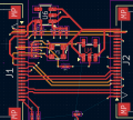
Layer one looks like this:
1773375029264.png


Y1 is 24MHz oscillator U1 and U2 are V1.5 and V2.8 voltage regulators together with decoupling capacitors.

Focusing on MIPI CIS:
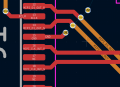
1773375140386.png

You can see a row or 4 vias, the 2 inner ones are to pass diff pair to 3rd layer the outer 2 are to provide return current path to ground. On the far left side you can also see the XCLK 24 mhz signal that is on the same layer, hope they won't interfere.

I would appreciate any feedback for my layout @Rf300, @drjohsmith @MrAl thanks in advance! :)
 

MrAl

Joined Jun 17, 2014
13,765
Thanks @drjohsmith, very informative.
I have corrected my first layout with key modifications:
- moved from 2 to 4 layers
- removed flood ground planes all together
- added ground vias next signal vias
- moved stuff around to provide short paths for key signals

My PCB stackup looks as follows:
L1 - all components (2x V.regulators + 24mhz oscilator + bunch of passive components), 2 pairs of MIPI CSI differential signals
L2 - solid GND plane and nothing else
L3 - one more MIPI CSI differential pair that didn't fit on L1 + 24mhz clock + I2C (SDA, SCL) + 1V5 via line
L4 - solid GND plane only

Layer one looks like this:
View attachment 364597


Y1 is 24MHz oscillator U1 and U2 are V1.5 and V2.8 voltage regulators together with decoupling capacitors.

Focusing on MIPI CIS:
View attachment 364598

You can see a row or 4 vias, the 2 inner ones are to pass diff pair to 3rd layer the outer 2 are to provide return current path to ground. On the far left side you can also see the XCLK 24 mhz signal that is on the same layer, hope they won't interfere.

I would appreciate any feedback for my layout @Rf300, @drjohsmith @MrAl thanks in advance! :)
Hi,

I wish I could help more but it's been a fairly long time since I did a board layout, even simpler low frequency ones.
These days I have a tendency to dive into theory over practice. Theory always piqued my interest even though I did a lot of practical circuits on the job and at home as a hobby, especially when I needed a product that was not available anywhere on earth.

I've used various techniques in the past, but when I worked in the industry we would send the schematic out to be made into a PC board and they would send it back to me. I would then go over the layout they chose and adjust certain trace runs and look for the basic wiring errors. It was quite a challenge as one of the boards measured something like 18 inches by 36 inches (it was a huge board). All the traces had to be carefully checked. After that we send the board out to be actually made, and then we would get 1 or more boards back that were completed. Any adjustments after that had to be done with buss wire and Teflon tubing. We usually did pretty good with that though, so it was rare that we had to do any additional adjustments later.
 
Last edited:

drjohsmith

Joined Dec 13, 2021
1,630
Thanks @drjohsmith, very informative.
I have corrected my first layout with key modifications:
- moved from 2 to 4 layers
- removed flood ground planes all together
- added ground vias next signal vias
- moved stuff around to provide short paths for key signals

My PCB stackup looks as follows:
L1 - all components (2x V.regulators + 24mhz oscilator + bunch of passive components), 2 pairs of MIPI CSI differential signals
L2 - solid GND plane and nothing else
L3 - one more MIPI CSI differential pair that didn't fit on L1 + 24mhz clock + I2C (SDA, SCL) + 1V5 via line
L4 - solid GND plane only

Layer one looks like this:
View attachment 364597


Y1 is 24MHz oscillator U1 and U2 are V1.5 and V2.8 voltage regulators together with decoupling capacitors.

Focusing on MIPI CIS:
View attachment 364598

You can see a row or 4 vias, the 2 inner ones are to pass diff pair to 3rd layer the outer 2 are to provide return current path to ground. On the far left side you can also see the XCLK 24 mhz signal that is on the same layer, hope they won't interfere.

I would appreciate any feedback for my layout @Rf300, @drjohsmith @MrAl thanks in advance! :)
Looking good.
It would be normal to have the board layeres symetrical around the center ..
Layer 1 and 4 want to have the same sort of amount of copper .
Same goes for layer 2 and 3

The visa look very small compared to the pad / track size. Could be a printing issue.

Talk to whom your using to build PCB
They will have preferred stock of material and standard stack arrangement
 

Thread Starter

mondo90

Joined May 16, 2025
126
Thanks for the feedback. I have increased all vias sizes to 0.4mm diameter and 0.2mm hole.
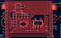
I am also thinking about adding a ground pour on part of the top layer like this:
1773424124452.png

Note it ends at the high speed diff pairs. The rationale is to provide lower impedance for all these votage regulators and decoupling capacitors + better EMI shielding + thermal relief (it will draw a bit of current).
Although I am not sure if in this scenario I still need that many GND VIAs as I have.. probably not
 

Thread Starter

mondo90

Joined May 16, 2025
126
Although in a second look I think this is actually a bad idea. First it will cause impedance discontinuity of differential pairs. Second I have several voltage domains, I am afraid it may mess it up, with ground bounces
 
Top