Facebook
 Google
 GitHub
 Linkedin
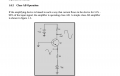
I snipped this from the NEETS module 8 , for amplifiers. (navy electronics education and training series).
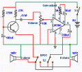
This image is the books basic concept schematic for a class AB amplifier, but what I'm talking about is the input for the signal being on the emitter, and the base being grounded.
Is this a possible circuit? I see it nowhere else, the logic doesn't seem to work out, but then, the navy has signed and dotted this module so perhaps it's a conspiracy to promote closed-culture and exclusive behavior, or perhaps it's just someone who thinks they don't get paid enough so maliciously wrote the texts, either way to me, with my untrained eye, it does look inaccurate.
Attachments
-
 72.1 KB Views: 61
.jpg")