Is it ok to have copper pours with deviations and edges like this?

Thread Starter

tdengineer

Joined Oct 21, 2025
36
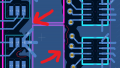
The Vias anti padding is creating these crazy edge shapes on my copper pours and I don't know if thats ok to send off to a manufacturer

How is this supposed to be done professionally?
 

Attachments

Ian0

Joined Aug 7, 2020
13,097
For the right-hand side problem, firstly use the align command to align all the vias. Then draw a rectangular keep-out zone around them, telling it to keep out zone fills only.

for the left-hand side problem, don’t put any track to the ground pad, let the filled zone do it for you. You can use solid fills instead of thermal reliefs. The another keep-out zone around pin 2s and pin 5s of that row of ICs should neaten it up.

But the manufacturer doesn’t care. I just like it to look tidy, even though no-one ever looks at it.
 
Last edited:

ronsimpson

Joined Oct 7, 2019
4,646
You appear to use traces to connect ground pads to the ground plane. I let the computer do that. Only add traces if the computer does a bad job.
I set the clearance for the plane to much less than what you have. (1/2 for an example)
 

Thread Starter

tdengineer

Joined Oct 21, 2025
36
For the right-hand side problem, firstly use the align command to align all the vias. Then draw a rectangular keep-out zone around them, telling it to keep out zone fills only.

for the left-hand side problem, don’t put any track to the ground pad, let the filled zone do it for you. You can use solid fills instead of thermal reliefs. The another keep-out zone around pin 2s and pin 5s of that row of ICs should neaten it up.

But the manufacturer doesn’t care. I just like it to look tidy, even though no-one ever looks at it.
I love the advice of aligning the vias i have ocd and I like perfection and alignment
 

MrChips

Joined Oct 2, 2009
34,628
I agree with ron. It would appear that you have not named the flood plane as GND.
Do this and let the layout program connect the GND.
 
Top