ir2113 HO output wave problem

Thread Starter

robousa

Joined Mar 25, 2019
6
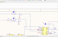
hi buddies...i want to drive irfz44 mosfet with ir2113 gate driver..for HIN and LIN input i used NOT GATE and schmitt trigger for create dead time but in output of HO.. my square wave have additional edge...below picture


this edge increase my losses...What is my mistake?...tnx
 

Attachments

Last edited:

Alec_t

Joined Sep 17, 2013
14,280
Welcome to AAC!
Without seeing a schematic of your complete circuit we can only guess what the mistake might be.
 

Alec_t

Joined Sep 17, 2013
14,280
What are the values of all the components shown?
What waveforms are driving D1 and U1c?
What gate resistors are you using?
 

Thread Starter

robousa

Joined Mar 25, 2019
6
What are the values of all the components shown?
What waveforms are driving D1 and U1c?
What gate resistors are you using?
tnx

input freq value is 15khz square wave with equel duty cycle......c1 and c2 value is 1nf.....R1 and R2 value is 2.2k ......U1 IS SN74HC14D..Hex Schmitt-Trigger Inverter
d1 ana d2 1n4148
FET gate resistor value is 8.2 ohm
 

Alec_t

Joined Sep 17, 2013
14,280
i used NOT GATE and schmitt trigger for create dead time
U1c merely provides polarity inversion: it does not introduce any significant dead time.
Why are you using R1,C1,R2,C2? Normally you would want fast switching of the FET gates.
 

Thread Starter

robousa

Joined Mar 25, 2019
6
U1c merely provides polarity inversion: it does not introduce any significant dead time.
Why are you using R1,C1,R2,C2? Normally you would want fast switching of the FET gates.
u1c introduce invert polarity wave for HIN input

R1 ,R2,C1,C2 to cause slope wave and when this wave crossing schmitt trigger it cause dead time....the rate of dead time depend on value of c1 and r1
 

Alec_t

Joined Sep 17, 2013
14,280
Here's a LTspice simulation result using the values you've given, assuming your 'equal duty cycle' means 50% high/50% low. Note that the RC slopes don't result in dead time between the HIN and LIN waveforms.
HIN-LIN.PNG
 

Thread Starter

robousa

Joined Mar 25, 2019
6
Here's a LTspice simulation result using the values you've given, assuming your 'equal duty cycle' means 50% high/50% low. Note that the RC slopes don't result in dead time between the HIN and LIN waveforms.
View attachment 173545
tnx..thats right...but according to data sheet the input of HIN AND LIN have schmitt trigger

my wave after crossing R1,R2,C1,C2


output of ir2113 HO AND LO


Alec_t

Joined Sep 17, 2013
14,280
The first scope shot waveforms would need the polarities of diodes D1 and D2 to be reversed, compared to what is shown in post #3.
What loads are connected to the FETs being switched by HO and LO?
If I'm reading your scope shots correctly you have channel 1 AC-coupled, channel 2 DC-coupled, and both channels offset by different amounts from zero. Why? It makes waveform comparisons more difficult.
If channel 1 is 100V/div, HO peak-to-peak seems to be about 260V. Is that right? It is inconsistent with the schematic.
 

Thread Starter

robousa

Joined Mar 25, 2019
6
What loads are connected to the FETs being switched by HO and LO?
the first shot have power supply on mosfet but in second shot no supply on FET....i think that the problem in schmitt trigger of ir2113 ...i try to use external sch trigger
 

Alec_t

Joined Sep 17, 2013
14,280
the first shot have power supply on mosfet but in second shot no supply on FET.
The FETs obviously can't switch on without a power supply. Unless the source pin of the high-side FET is being toggled high and low, the bootstrap capacitor won't raise the VB pin of the IC sufficiently to give reliable switching of the high-side FET. Perhaps that accounts for the problem you are experiencing. You can expect a step in the HO waveform, as a consequence of the dead time and the bootstrap operation.

Edit:
Here's a sim showing the step :-
Ho-Lo.PNG
 
Last edited:

danadak

Joined Mar 10, 2018
4,057
Just as a future ref a number of processors these days have dead time
configurable capability in their PWM implementation.

RC approaches suffer from serious drift due to T and V changes that
alter the timing. Unlike processors that depend on a clock which is rel-
atively stable compared to RC approaches.


Regards, Dana.
 

s42255

Joined Mar 28, 2021
1
The FETs obviously can't switch on without a power supply. Unless the source pin of the high-side FET is being toggled high and low, the bootstrap capacitor won't raise the VB pin of the IC sufficiently to give reliable switching of the high-side FET. Perhaps that accounts for the problem you are experiencing. You can expect a step in the HO waveform, as a consequence of the dead time and the bootstrap operation.

Edit:
Here's a sim showing the step :-
View attachment 173717
Which software are you using?
 

Alec_t

Joined Sep 17, 2013
14,280
Welcome to AAC! Do you realise you are posting in a 2-year old thread?
The simulation software is LTspice, a free download from Analog Devices.
 
Top