IR2011 High side toff too slow (400ns)

Thread Starter

JulieA

Joined Feb 6, 2022
12
Hello,
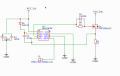
I am making an ESC for 75v motor (7KW). To achieve that I am testing the gate driver IR201, especially the most problematic part the High side (see my schematic in attachment). The Ton is quite near the datasheet 100ns (instead of 80ns) , but the Toff is 400ns instead of 60ns.
I tried with different capacitor values (from 1µF to 47µf) but the result is always the same.
(The timing of Hin si 400µs High and 4000µs Low)

Does somebody encounter this problem?

Great regards,
Julie
 

Attachments

ronsimpson

Joined Oct 7, 2019
2,985
How are you measuring the turn off time? With only 1A I think the turn off time will be slow.
What MOSFET are you using? I can not find a data sheet.

Why a 75V motor on a 24V supply? with only 10% duty cycle?
 
Last edited:

crutschow

Joined Mar 14, 2008
34,280
Why are you using the NMOS as high side switch?
Because N-MOSFETs are cheaper than P-MOSFETs for the same current rating.

The gate driver IR201 has a built-in bootstrap driver to generate a gate voltage nearly twice the supply voltage to turn on the N-MOSFET.
 

Thread Starter

JulieA

Joined Feb 6, 2022
12
How are you measuring the turn off time? With only 1A I think the turn off time will be slow.
What MOSFET are you using? I can not find a data sheet.

Why a 75V motor on a 24V supply? with only 10% duty cycle?
Hello,
I am mesuring the Toff time
How are you measuring the turn off time? With only 1A I think the turn off time will be slow.
What MOSFET are you using? I can not find a data sheet.

Why a 75V motor on a 24V supply? with only 10% duty cycle?
Hello,
I am mesuring the Toff at Ho output (it does the same result Toff mesuring R1)
the mosfet is fdp2D9n12c (link https://www.mouser.fr/datasheet/2/308/1/FDP2D9N12C_D-2312595.pdf)
24v because my power suppy does not exceed for the moment 24v
10% of cycle : why not ?

Regards,
Julie
 

ronsimpson

Joined Oct 7, 2019
2,985
I am mesuring the Toff time
The data sheet measures off time at 95A and you are measuring at 1A. The output capacitance of the MOSFET is 7910pf typical and 12883pf max. You need to discharge this cap with a 27 ohm resistor. That is part of the problem.

Are you looking at the Gate when you measure switching time. (scope probe on Gate??) That will really slow the part.
 

Thread Starter

JulieA

Joined Feb 6, 2022
12
The data sheet measures off time at 95A and you are measuring at 1A. The output capacitance of the MOSFET is 7910pf typical and 12883pf max. You need to discharge this cap with a 27 ohm resistor. That is part of the problem.

Are you looking at the Gate when you measure switching time. (scope probe on Gate??) That will really slow the part.
"You need to discharge this cap with a 27 ohm resistor" : I thought that was the gate driver job, to discharge the gate capacitor. I'am looking at the ouput of the gate driver, not a the gate.
 

ronsimpson

Joined Oct 7, 2019
2,985
I thought that was the gate driver job, to discharge the gate capacitor. I'am looking at the ouput of the gate driver, not a the gate.
The gate driver discharges the Capacitance G-S. The capacitance from D-S is charged/discharged by the MOSFET and the load, not the driver.
 

Orson_Cart

Joined Jan 1, 2020
90
To measure the top side gate drive signal - you need an isolated channel scope - if you look at Ho w.r.t. ( with respect to ) gnd, then you see the mid point + gate drive, assuming the chip & mosfet are OK, you should see this waveform drop quickly for the first part ( the gate drive going low ) but after that the residual voltage you see is entirely dependent on the load & the capacitance of the devices, eventually the low side gate drive will go high pulling the mid point to ground - so you see your delay you think you are seeing - could well be that - always a good idea to post lots of oscillograph shots to make it easier for readers to diagnose.
 

Thread Starter

JulieA

Joined Feb 6, 2022
12
The gate driver discharges the Capacitance G-S. The capacitance from D-S is charged/discharged by the MOSFET and the load, not the driver.
Thaks for the answer. The capacitance from D-S is charged (when the mosfet is off) through the R1 resistance (connected beetween , Mosfet Source and ground) . But I don't understand how could The capacitance from D-S is really discharged ?

Note perhaps a clue to my problem , before putting D1 in parrallel of the resistance between HO and the Mosfet gate the Toff was worst 2µs , introducing D1 acts like a shunt for the discharge of the capacitance from D-S , so its seems that gate driver make somme job for the the discharge
 

Thread Starter

JulieA

Joined Feb 6, 2022
12
Adding a scope probe to the Gate Driver output or the Gate will slow down the switching times. (top side driver)
For the low side this scope probe has little effect.
Ok but the Toff measurement at the load gives the same result , I thing that for a 27Ohm resistance the scope probe has no effet
 

Thread Starter

JulieA

Joined Feb 6, 2022
12
To measure the top side gate drive signal - you need an isolated channel scope - if you look at Ho w.r.t. ( with respect to ) gnd, then you see the mid point + gate drive, assuming the chip & mosfet are OK, you should see this waveform drop quickly for the first part ( the gate drive going low ) but after that the residual voltage you see is entirely dependent on the load & the capacitance of the devices, eventually the low side gate drive will go high pulling the mid point to ground - so you see your delay you think you are seeing - could well be that - always a good idea to post lots of oscillograph shots to make it easier for readers to diagnose.
I have a screen capture of the voltage on the load resistance with 100ns resolution
 

Attachments

Top