IGBT H-Bridge Design Question

Thread Starter

weedoublewide

Joined Apr 25, 2020
15
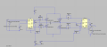
I'm having some issues getting my PWM signals timing tuned in and not overlapping Even with an time-delay added in, I seem to be getting some shoot through current, well alot (+200A), on the supply voltage source.

It's a great possibility that I'm missing something as well.

Below is the link to the lib files I found via online.
http://bordodynov.ltwiki.org/

I've attached a picture and the .ASC file

If anyone has some expertise with this, I'd greatly appreciate your help.

Thank you
 

Attachments

Bordodynov

Joined May 20, 2015
3,179
In order not to have transistors switched on at the same time, the time of switched on state must be less than 50% of the period.
I didn't like the right side of the circuit. You controlled the lower transistor output for the upper transistor and the upper transistor output for the lower one. I rearranged the shutters and swapped the signal sources. Circuit outputs are not equal! Use the chips for their intended purpose.
 

Thread Starter

weedoublewide

Joined Apr 25, 2020
15
In order not to have transistors switched on at the same time, the time of switched on state must be less than 50% of the period.
I didn't like the right side of the circuit. You controlled the lower transistor output for the upper transistor and the upper transistor output for the lower one. I rearranged the shutters and swapped the signal sources. Circuit outputs are not equal! Use the chips for their intended purpose.
I get the first part. My understanding of hi side and lo side drivers was backwards, now that I've done some more reading on it, it makes more sense.

I did notice that the high side driver is going to have higher than source voltage on the gate, that's why theres 60V leading into the gate. While theres only 15 on the lo side.

Do you mean even with the changes you made, the circuit outputs aren't equal? I was under the impression these chips would suffice, at least for testing and building a stronger foundation of understanding. At least before I rip into the lab and start building stuff I obviously don't understand lol.

And maybe I'm not understanding full what you mean by "intended purpose"? When wired correctly is it not doing the job its suppose to do?

From a afar, they seem easy. Start digging into it and it gets a little more fuzzy
 

Bordodynov

Joined May 20, 2015
3,179
I did the right thing. Take your original schematic and see what happens on the transistor gates. Then take the circuit I corrected and look at the transistor gate signal, too.
I corrected your circuitry. What more do you want from me?
If you get any weirdness in your simulation, look at the signals you're getting. It might rule out the need to ask other people questions. So I'm urging you to be self-sufficient.
 

Thread Starter

weedoublewide

Joined Apr 25, 2020
15
I did the right thing. Take your original schematic and see what happens on the transistor gates. Then take the circuit I corrected and look at the transistor gate signal, too.
I corrected your circuitry. What more do you want from me?
If you get any weirdness in your simulation, look at the signals you're getting. It might rule out the need to ask other people questions. So I'm urging you to be self-sufficient.
And thank you very much for helping me, you don't know how much I appreciate it.
I was just using the opportunity to learn as much as I could for you before this thread closing, my apologizes for trying to pick your brain.

Again thank you,

double
 
Top