Ideas for Designing 3 Phase Power Stage For BLDC/ACIM Motor

TechWise

Joined Aug 24, 2018
151
I'm late to this thread, so I haven't yet caught up on what has happened before this latest test. Couple of questions...
  1. How are you probing your gate signals? You need to make sure that the issues you're seeing actually exist and that they're not ringing of the probe or noise that you've picked up. Effective probing in a harsh environement like a power converter is not easy.
  2. The bottom image shows the high and low side gate signals. Have you inserted a dead band between the two? Not inserting a dead band is a sure way to destroy your switches and also a sure way to introduce current spikes which will affect your measurements. This will be easy to implement on the F28069.
 

Thread Starter

ashkarmalik

Joined Jul 1, 2012
115
I'm late to this thread, so I haven't yet caught up on what has happened before this latest test. A couple of questions...
  1. How are you probing your gate signals? You need to make sure that the issues you're seeing actually exist and that they're not ringing of the probe or noise that you've picked up. Effective probing in a harsh environment like a power converter is not easy.
  2. The bottom image shows the high and low side gate signals. Have you inserted a dead band between the two? Not inserting a dead band is a sure way to destroy your switches and also a sure way to introduce current spikes which will affect your measurements. This will be easy to implement on the F28069.
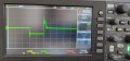
1) I am probing the signals from the MOSFET gate leads directly and connecting the ground clips on the ground trace coming on the PCB itself.
2) I haven't placed any dead time between the high side and low side MOSFETs. I think I have to place that now.
 

TechWise

Joined Aug 24, 2018
151
1) I am probing the signals from the MOSFET gate leads directly and connecting the ground clips on the ground trace coming on the PCB itself.
2) I haven't placed any dead time between the high side and low side MOSFETs. I think I have to place that now.
Assuming you're using isolated probes, I would probed directly with the positive clip on the gate pin of the MOSFET and the negative clip on the source pin of the MOSFET. Be very careful not to short anything out with the probe clips and also do not use this approach on the high side switch without isolated probes!

It is essential that you insert a dead-time in your gate drive signals. There will be an example in the C2000Ware for the F28069 that shows you how to do this.
 

Thread Starter

ashkarmalik

Joined Jul 1, 2012
115
Assuming you're using isolated probes, I would probe directly with the positive clip on the gate pin of the MOSFET and the negative clip on the source pin of the MOSFET. Be very careful not to short anything out with the probe clips and also do not use this approach on the high side switch without isolated probes!

It is essential that you insert a dead-time in your gate drive signals. There will be an example in the C2000Ware for the F28069 that shows you how to do this.
Thanks for the feedback, I have done the proposed settings. And injected a small dead band.
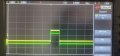
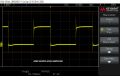
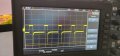
First Image is of H-Bridge Output with a resistive load conected.
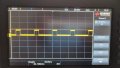
Second Image is of High Side and Low Side Mosfet Gate Pins.
 

Attachments

Last edited:

TechWise

Joined Aug 24, 2018
151
Thanks for the feedback, I have done the proposed settings. And injected a small dead band.
First Image is of H-Bridge Output with a resistive load conected.
Second Image is of High Side and Low Side Mosfet Gate Pins.
If that second image is of the high side and low side MOSFET gate pins then they are both turned on at the same time!
 

Thread Starter

ashkarmalik

Joined Jul 1, 2012
115
If that second image is of the high side and low side MOSFET gate pins then they are both turned on at the same time!
WhatsApp Image 2020-09-20 at 1.46.47 PM.jpeg
High Side Mosfet WaveForm With Respect to Drain Terminal. and At Gate.
6.png

Bottom Side Mosfet Waveform With respect to Ground.

After Running for 1 Minute the Lower side mosfet failed (One failed of the two)

4.png

Output Wave form across resistive load.

10.png
 
Last edited:

TechWise

Joined Aug 24, 2018
151
You need to measure the Gate to Source voltage for the high side switch and the low side switch at the same time on the scope. Verify that they are complementary, active high with a deadband inbetween. You should check your gate signals in this way before you even think about energising the DC bus. There's no need to be destroying MOSFETs at this stage. Check things in a logical order, starting with the gate drive signals when the DC link is at 0V.
 

Thread Starter

ashkarmalik

Joined Jul 1, 2012
115
You need to measure the Gate to Source voltage for the high side switch and the low side switch at the same time on the scope. Verify that they are complementary, active high with a Deadband in-between. You should check your gate signals in this way before you even think about energizing the DC bus. There's no need to be destroying MOSFETs at this stage. Check things in a logical order, starting with the gate drive signals when the DC link is at 0V.
Thank you for your reply, I wanted to know one thing, I don't know If I am doing something wrong, Please verify the waveforms that I am creating.
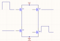
Diagonal Mosfets are kept off.
 

Attachments

Thread Starter

ashkarmalik

Joined Jul 1, 2012
115
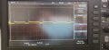
Waveform across h-bridge output.
spikes.jpeg
Mosfet That I am using are IRF540N so Maximum they can hold 110v DC

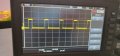
High Side Gate Voltage are 18.7v and It seems to be very high. I Guess inductive spikes are creating these levels! (Gate-Source)

highside.jpeg

This Is High Side Gate Wave form (Gate-Drain)
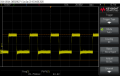
highside-gate drain.jpeg After adding Fly back diodes in h_bridge the waveform at High side_gate_source are as below

after_diode_Hidhside_gate_source.jpeg
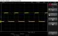
After adding Fly back diodes in h_bridge the waveform at High side GATE-DRAIN are as below

after_diode_Hidhside_gate_drain.jpeg

What I see is the voltages across the Gate are Climbing to about 20v Insted of 12v that I have supplied to gate drivers.
 
Last edited:
Top