Facebook
 Google
 GitHub
 Linkedin
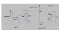
And no he did not built an audio amplifier or RF amp using these specifications as far as I know.The teacher just gave the question which I posted earlier. And he did not give the load resistance. But just said to build a class B push pull amplifier with transformer coupled at both input and output with a load current of 1A using TIP 31 and TIP 32. I think now the question is quite clear. I said center tapped earlier because I thought it was the only way to incorporate a transformer in the circuit. I am sorry if it misguided you.
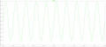
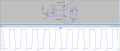
I need to simulate a class B push pull amplifier with center tapped transformers to get 1A load current.
- Thread starter Mustaqeem Tariq
- Start date