Facebook
 Google
 GitHub
 Linkedin
hello,
I need help to understand this circuit
3 to 8 decoder
2 to 4 decoder
8 bit instruction register
look the instruction register. I think first four bit specify opcode ,then two bit specify destination ,and then two bit specify source
now I want to modify that circuit I want to add accumulator , registers and Ram memory
how to do , I don't understand how to connect another component ?
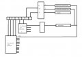
I need help to understand this circuit
as per my knowledge there are three component

3 to 8 decoder
2 to 4 decoder
8 bit instruction register
look the instruction register. I think first four bit specify opcode ,then two bit specify destination ,and then two bit specify source
now I want to modify that circuit I want to add accumulator , registers and Ram memory
how to do , I don't understand how to connect another component ?