Facebook
 Google
 GitHub
 Linkedin

ebeowulf17
- Joined Aug 12, 2014
- 3,307
Yes, that was it!@ebeowulf17
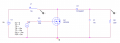
I believe this is the case with the schematic originally posted, the inverting converter. However, if my understanding is correct, with the boost converter D1 is switched around to allow current flow such that the solar panel can power the load despite the FET being in the off state. I attached a schematic of this circuit in an earlier reply.
Hope this helps, correct me if I'm wrong. Thanks!
I apologize to both you and @ebp. I was reading a little too fast earlier and totally missed that we were discussing a different schematic now. Everything makes sense again. I'll try to slow down and read more carefully before making more comments and asking silly questions. Thanks!