How to simulate/represent a GPIO in a circuit?

Thread Starter

idkq

Joined Jan 29, 2022
9
Beginner here. I always get confused on how GPIO set as input on microcontrollers should be represented and simulated on a circuit.

Example

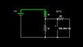
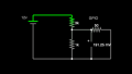
Take this simple voltage divider for example:

circuit-20220204-2116.png

If I have a 3k and 1k resistor, Vin = 12v, then Vout = 3.06v which is ok because it is below the max voltage of the GPIO for ESP32 microcontroller which is 3.3v. So working with voltage is easy.

But current is tricky. The questions I want to answer with this simulation is mainly on the value of the resistors:

- Does the current exceed the max rating for the microcontroller GPIO (ESP32 in the case)?
- Is the current enough for the ADC to be able to read the voltage?

So how can I simulate the current going inside the GPIO to answer these questions?

For example why 3k and 1k and not 300 and 100 ohms? Or why not 30k and 10k instead? Or why not 1M and 3M?

Bottom line, how can I draw the circuit above to represent an input ADC GPIO readings?

Circuit: https://tinyurl.com/y8b255u9
 

Attachments

MrChips

Joined Oct 2, 2009
34,628
You are on the wrong track.

An ADC input pin is generally a high resistance, typically 100k-1MΩ. It does not sink or supply current. The key parameter you need to look up is the leakage current which typically is in the 1μA range.

The general rule of thumb is any driver circuit should have a resistance that is 10 times lower than that of the receiving end. In this way any loading effect will be below 10%.

For example, if the ADC input resistance is 100kΩ then the source resistance should be lower than 10kΩ.

To answer part of your question, why not go to 100Ω or even 1Ω in a voltage divider?
You do not go too low because you are now putting a heavy load on the source which now has to drive higher current.

Bottom line: You want the voltage divider output resistance to be as high as possible while still lower than 1/10 of the receiver's input resistance.
 

Papabravo

Joined Feb 24, 2006
22,058
The simulation of a digital GPIO involves a bit more than resistors. You should think of an output device that has 3-states: Low, High, and High Impedance. The input device, connected to the GPIO consists of a hig impedance buffer with hysteresis, also called a Schmitt Trigger. Most processor datasheets will have a pretty comprehensive block diagram of a GPIO port.
 

Thread Starter

idkq

Joined Jan 29, 2022
9
Many thanks for you answer. Quick follow ups

An ADC input pin is generally a high resistance, typically 100k-1MΩ. It does not sink or supply current.
So a high/low current is not an "issue" for the pin?

The key parameter you need to look up is the leakage current which typically is in the 1μA range.
What do I use the leakage current for?

To answer part of your question, why not go to 100Ω or even 1Ω in a voltage divider?
You do not go too low because you are now putting a heavy load on the source which now has to drive higher current.
Bottom line: You want the voltage divider output resistance to be as high as possible while still lower than 1/10 of the receiver's input resistance.
So I guess it is a good practice to keep resistance high (up to the 1/10 rule), but it would not necessarly damage the port to go lower?
 

Papabravo

Joined Feb 24, 2006
22,058
I looked through two ESP32 documents looking for a block diagram of an I/O port and could not find one. Here is one for a Microchip part.

1644030730659.png
Notice the two diodes connected to the I/O pin and to the power(VDD) supply and GROUND (VSS). These diodes prevent the voltage on the pin from going too far above the power supply voltage or too far below GROUND. The TRISx signal is what determines if the output is High Impedance, or controlled by the output of the Flip-Flop.
 

eetech00

Joined Jun 8, 2013
4,704
HI

I've been working on this for some time now. It still isn't finished yet.
It simulates an Arduino GPIO pin, including boot behavior, tri-state mode, PWM and other electrical specs.
I'm making one for PIC also.

1644039137542.png
 
I looked through two ESP32 documents looking for a block diagram of an I/O port and could not find one. Here is one for a Microchip part.

View attachment 259702
Notice the two diodes connected to the I/O pin and to the power(VDD) supply and GROUND (VSS). These diodes prevent the voltage on the pin from going too far above the power supply voltage or too far below GROUND. The TRISx signal is what determines if the output is High Impedance, or controlled by the output of the Flip-Flop.
what is the source of this picture?
 

Papabravo

Joined Feb 24, 2006
22,058
what is the source of this picture?
In my post on the subject, I said:

"Here is one for a Microchip part. "​
I don't remember which PIC datasheet I grabbed the screen clip from, but it was probably a member of the mid-range PIC16F family of parts. Almost all I/O ports for modern microcontrollers follow the same general approach. If you can find one for an ESP32, you should post it here.
 
Top