 Facebook
 Google
 GitHub
 Linkedin
Hi,
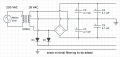
In an ongoing project I've made a solid state relay for muting audio speakers because of turn-off thump. The large filter capacitors of the power supply will be by-passed with a full wave rectifier to be able to detect turn-off before the main supply voltage collapses. Please refer to the attached diagram. This by-pass should yield about 26 VDC.
I want to use this 26 VDC signal to switch on/off the 555 that drives the relay. But how do I pull the RESET pin below 0.7 V? With a 2N3906 I can get it to work in a simulation if the base resistor value is low enough (<1k Ω). But since the voltage drop across the 2N3906 is around the RESET threshold value this will probably not be The Right Way.
Swapping the 2N3906 with a p-channel enhancement MOSFET makes things worse which I don't understand. LTSpice has the BSS84, I have some BS250s. They seem close enough. The RESET voltage drops to only ~2.4 V. If the Rds_on is about 10 Ω and R3 is 10k Ω, why is V(n002) not 15*10/10k = 0.015 V?
Is it a problem to drive the base/gate with a voltage much higher than the collector/source voltage? I think Vcbo does not apply here as the junction is reverse biased.
If you have a suggestion for a better way to do this, I'm open to suggestion! But it would need to work with the existing 555 circuit.
Thanks
Attachments
-
 32.8 KB Views: 23
 -
 27.3 KB Views: 42
 -
2.2 KB Views: 5
-
2.2 KB Views: 4
")


