Facebook
 Google
 GitHub
 Linkedin

Hi everyone,
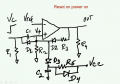
I'm trying to understand this circuit (attached image) as part of an experiment I'm running, based on this video:
I understand basic comparator operation and the standard Schmitt trigger configuration (positive feedback creating hysteresis around V+ = V-), but this particular circuit has extra components I can't fully make sense of. I'd really appreciate a breakdown of what each block is doing and why.
Specifically:
I'll attach the schematic (hand-drawn) . Any explanation of the signal flow at power-on and during a "set/reset" transition would be hugely appreciated.
Thanks in advance!
I'm trying to understand this circuit (attached image) as part of an experiment I'm running, based on this video:
I understand basic comparator operation and the standard Schmitt trigger configuration (positive feedback creating hysteresis around V+ = V-), but this particular circuit has extra components I can't fully make sense of. I'd really appreciate a breakdown of what each block is doing and why.
Specifically:
- C1 and D1 are connected between the Vc line and the V+ node. What role does this RC/diode combination play?
- D2 and R3 form a path from OUT back to V+. This looks like positive feedback, but through a diode rather than a plain resistor?
- D3, R5, C2, D4, and Vcc What is each component's function here (particularly D4)?
- R2 ties V+ to ground, and R4 is on the output. What are these two resistors doing in context ?
I'll attach the schematic (hand-drawn) . Any explanation of the signal flow at power-on and during a "set/reset" transition would be hugely appreciated.
Thanks in advance!
Attachments
-
 1 MB Views: 10