Facebook
 Google
 GitHub
 Linkedin
Hi Folks,
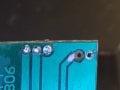
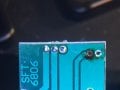
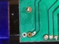
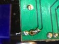
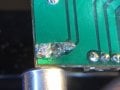
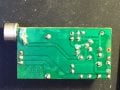
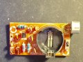
Hope this is an appropriate post for this section. I've been working my way up on learning rf circuits and building them by doing small rf boards- transmitters, receivers, etc. One of the small projects I just put together this am was a small transmitter kit from China. The circuit uses an electret condenser mic with 2 leads and next to it is a flat coin type battery holder. I survey the board quickly to get a general idea of what order to place the components, as the instructions were in Chinese, and I was working from the circuit schematic and diagram. The project went together very well, and after I was done, I just did a last survey of the solder joints and found a cold one, where I had to resolder the mic early on, as you had to bend the mic over the edge of the board to allow the battery holder to set on the board. As I unsoldered and resolder the mic after bending it, I noticed that one of the joints had lifted off the board and no amount of solder would reconnect it. It looks like the copper pad has lifted off the trace. What are my options if any, to get the one lead of the mic reattached to the adjacent trace, without a copper pad- sandpaper or scrape some of the trace covering off?
Thanks very much and any suggestions are appreciated.
Dave
Fort Collins, CO