How to design a H bridge with N-MOSFETs and control them?

Thread Starter

Jimpes

Joined Jan 12, 2017
8
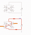
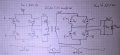
Here the schematic and my asc file.
I have to use a output capacitor to filter the voltage.
But now I have a power dissipation that is not usual for an MOSFET rectifier.
This circuit lose about .8 volts, therefor I can use a simple diode H-Bridge with schottkey diodes.

I hope for helping ;)
Thanks
 

Attachments

crutschow

Joined Mar 14, 2008
38,668
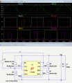
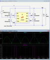
Below is a simulation of the LT4320 bridge circuit which controls the Vgs of the 4 N-MOSFETs as required.
As can be seen, the bottom MOSFETs can be on for 1/2 cycle but the top MOSFETs are on only when the input peak AC voltage V(2,1) is greater than the capacitor output voltage.
They must be turned off when the input voltage drops below the capacitor output voltage or the capacitor will drain back through the MOSFETs.

Thus you need two comparator circuits to monitor the voltage across the top MOSFETs and turn them off when the polarity is reversed, indicating the current through them is reversed.

And, although some non-overlap is shown between the two bottom MOSFET gate signals, it's not critical if they switch at the zero crossing of the AC waveform.

Thus my comment that this is not a simple circuit.
If you only have to drive a resistive load it's much simpler since you don't have to worry about current being fed back from the load.

upload_2017-1-15_23-31-56.png
 

Attachments

MrAl

Joined Jun 17, 2014
13,756
Hi,

Yeah that looks pretty good. That's probably the way i would do it too to make it simpler. You can see the dead time appear in the waveforms, but if you rather not think about it in that way that's fine too.

In the case of the "roll your own controller" i was suggesting that maybe we can measure the output and also measure the in coming sine wave, then only allow any mosfet to turn on when the input sine is greater than the output voltage (positive have cycle or less than for negative half cycles).
So for example, as the sine voltage is rising from 0 and say it is as 2.0v right now, if the output is 3.0v then we dont allow any turn on fo any mosfet. As the input rises to say 2.9v we still dont allow any mosfet to turn on, but as it climbs up to maybe 3.1v (0.2v above the output) then and only then we allow it to turn on. The input will then peak at some point, with the output still slightly lower, then it will start to fall, and say it reaches 2.9v with the output at 3.0v, then we disable all mosfets again. This might work up to maybe 20v or so. If we go too much higher then we'd probably have to go back to measuring the voltage across each diode to get the accuracy needed.
 

crutschow

Joined Mar 14, 2008
38,668
This is an interesting problem so I had to mull it over, but the best I could do with discrete parts is to use a bridge of half N-MOSFETs and half P-MOSFETs along with a couple of comparators.

Edit:The circuit is described in the reference here.
 
Last edited:

Thread Starter

Jimpes

Joined Jan 12, 2017
8
Hi

thanks a lot for your replys.

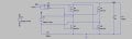
I attached a schematic plan that you can suggest what I mean.
Input voltage: 12V DC
then a Dc to AC inverter --> transformer 1:1 --> a AC to DC rectifier
all only with resistor, capacitor, opamps, N-MOSFETs, inductors, transformer
But no IC like this LT4320.

For the first step to control all Mosfets should take e.g. voltage sources (PWM or PWL ...)

Thanks for helping.
 

Attachments

MrAl

Joined Jun 17, 2014
13,756
This is an interesting problem so I had to mull it over, but the best I could do with discrete parts is to use a bridge of half N-MOSFETs and half P-MOSFETs along with a couple of comparators.
The LT spice simulation is shown below.
I used two comparators to control the gates of M2 and M4 to shut them off other then when the capacitor is charging to avoid any back current discharge of the capacitor through them.
The comparator senses when the respective sine-wave goes negative with respect to ground, indicating the cap is charging, and turns on the appropriate MOSFET
They are turned off otherwise, whenever the voltage is positive.

(Note that neither sinewave node goes significantly below ground (equal to the MOSFET drop from the current flow), the way the ground is connected in the circuit.)
-
-The MOSFETs are working properly since the measured output voltage is only a few mV below the peak sine voltage.

View attachment 118848
Hi,

Interesting circuit. With all mosfets off to start, how does the first mosfet, say M1, turn on?
Note that in real life we have a true floating input sine source while in simulation it could be ground referenced already to 1/2 Vpeaktopeak. Just something to check for, maybe we need to see the reverse diodes also.

Looks like a cool idea though.
 

crutschow

Joined Mar 14, 2008
38,668
Interesting circuit. With all mosfets off to start, how does the first mosfet, say M1, turn on?.
The initial output capacitor voltage is generated by current through the M2 and M4 P-MOSFET substrate diodes.
M1 and M3 are turned on by the AC voltage to their gates.
Note that in real life we have a true floating input sine source while in simulation it could be ground referenced already to 1/2 Vpeaktopeak. Just something to check for, maybe we need to see the reverse diodes also.
The circuit requires a floating AC source.
It will not work if the AC source is grounded.
If the AC source is grounded then the the bridge, load, and comparator common must all float.
 

MrAl

Joined Jun 17, 2014
13,756
The initial output capacitor voltage is generated by current through the M2 and M4 P-MOSFET substrate diodes.
M1 and M3 are turned on by the AC voltage to their gates.
The circuit requires a floating AC source.
It will not work if the AC source is grounded.
If the AC source is grounded then the the bridge, load, and comparator common must all float.
Hi,

It looks like it could work. What happened for me was when i first looked at it i had assumed all the mosfets were N channel because he had also specified that they had to be N channel. No big deal though :)
 

crutschow

Joined Mar 14, 2008
38,668
It looks like it could work. What happened for me was when i first looked at it i had assumed all the mosfets were N channel because he had also specified that they had to be N channel. No big deal though
Yup.
I couldn't see how to easily do the circuit with all N-MOSFETs. o_O
 

Thread Starter

Jimpes

Joined Jan 12, 2017
8
Hi

thanks a lot for your replys.

I attached a schematic plan that you can suggest what I mean.
Input voltage: 12V DC
then a Dc to AC inverter --> transformer 1:1 --> a AC to DC rectifier
all only with resistor, capacitor, opamps, N-MOSFETs, inductors, transformer
But no IC like this LT4320.

For the first step to control all Mosfets should take e.g. voltage sources (PWM or PWL ...)

Thanks for helping.
Do somewhere have an idea for a circuit?
at all for control this Mosfets?
 

MrAl

Joined Jun 17, 2014
13,756
Hi

thanks a lot for your replys.

I attached a schematic plan that you can suggest what I mean.
Input voltage: 12V DC
then a Dc to AC inverter --> transformer 1:1 --> a AC to DC rectifier
all only with resistor, capacitor, opamps, N-MOSFETs, inductors, transformer
But no IC like this LT4320.

For the first step to control all Mosfets should take e.g. voltage sources (PWM or PWL ...)

Thanks for helping.
Hi,

Well, you could design a regular controller but make the drivers with an 'enable' pin so that you can disable all mosfets with one signal. Measure the input, measure the output. When the input is less than the output, disable all mosfets drivers. When the input is greater than the output, enable all mosfets drivers. When the mosfets are enabled, the normal control takes over, which is turning on one set of 2 when the input is positive and the other set when the input is negative.
You could probably use comparators for the measurements.
 

crutschow

Joined Mar 14, 2008
38,668
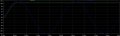
The difficulty with an all N-MOSFET bridge used for a rectifier or for any other bridge applications is that you need a voltage above the AC peak (bridge supply) voltage to turn on the top MOSFETs.
This usually means some sort of bootstrap driver for the bridge.
The LT4320 generates a gate output voltage for the top transistors that is above the peak of the sinewave and it's a puzzle to me how they do that without a large bootstrap capacitor.
Here's the simulation showing the gate voltage exceeding the peak input voltage by about 8V:
How do they do that? :confused:

upload_2017-1-17_13-47-30.png
 
Last edited:

MrAl

Joined Jun 17, 2014
13,756
The difficulty with an all N-MOSFET bridge used for a rectifier or for any other bridge applications is that you need a voltage above the AC peak (bridge supply) voltage to turn on the top MOSFETs.
This usually means some sort of bootstrap driver for the bridge.
The LT4320 has a gate output voltage for the top transistors that is above the peak of the sinewave and it's a puzzle to me how they do that without a large bootstrap capacitor.
Here's the simulation showing the gate voltage exceeding the peak input voltage by about 8V:
How do they do that? :confused:

View attachment 118942
Hi,

Isnt it obvious? They are using some of the background radiation left over from the Big Bang :)

Well from what we know about voltage boosters, we either need an inductor to boost the voltage or a capacitor to switch in series with some source voltage in order to increase the level of the drive voltage. We can be sure of this. What we dont know is what size they are using internally or if they are pulling another trick like taking the energy from one gate and using it later to drive the other gate. Another trick is to use an opto coupler with photovoltaic cells to increase voltage.
If we assume that they just use a capacitor, then it would be very likely that the capacitor would be a fairly small value, and that would mean the type of mosfet that they allow to be used would be limited, due to the limited available drive energy. This would have to be mentioned somewhere, in some way, or we would end up with designs that just dont work and nobody knows why.

We could do some tests like load the gate pin with some resistance, see when it starts to fail. stuff like that.

I looked around a little to try to find an internal diagram but could not find anything yet. I might look a little more later.
 
Top