How to choose error amplifier for a LDO?

Thread Starter

anhnha

Joined Apr 19, 2012
904
Hi.

With LDO (Low Dropout Voltage regulator) with input voltage ranges from 2 to 3.3V and output voltage is 1.8V.
From these specs, how should I choose error amplifier?
I am confused about how the input range relates to the error amplifier.
 

ErnieM

Joined Apr 24, 2011
8,415
Are you building your own LDO?

The input range is how much voltage your circuit has for power. Including the error amp.
 

Jony130

Joined Feb 17, 2009
5,601
Simply make sure that your error amp will work in linear region for 2V also. And will have as much gain as he can.
 

Thread Starter

anhnha

Joined Apr 19, 2012
904
Hi.
Thank you.
Are you building your own LDO?
Yes.
Simply make sure that your error amp will work in linear region for 2V also. And will have as much gain as he can.
My problem is here:
Vin: 2 to 3.3V
Vout: 1.8V

I am designing the error amplifier for this LDO.
For Vin from 2 to 2.9V: Vout = 1.8V
For Vin from 2.9 to 3.3V Vout follows exactly Vin: Vout = Vin

I need to increase the input range in which Vout = 1.8V. What specs of error amplifier that I need to change?
 

AnalogKid

Joined Aug 1, 2013
12,292
We need to see a schematic of the complete circuit. There are way too many possibilities to discuss without more information.

ak
 

Thread Starter

anhnha

Joined Apr 19, 2012
904
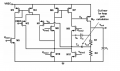
Hi. This is the circuit.


BTW, how can I choose Vbias1, Vbias2 and Vbias3 so that all transistors are in saturation?
 

Attachments

Thread Starter

anhnha

Joined Apr 19, 2012
904
I set Vbias1, Vbias2 and Vbias3 above the threshold voltages of M5, M8, M9, M10 and M11 a little and these transistors are in saturation.

However, some other transistors are not in saturation. How can I solve that?
Could you answer the question in post #4?
 

Thread Starter

anhnha

Joined Apr 19, 2012
904
My voltage gain is about 40dB. I need over 60dB. How can I increase that?
From the formula, I need to increase gm1, gm2. However, when I increase width of M1, M2 in a wide range, the voltage gain increase only 1dB.
 

Jony130

Joined Feb 17, 2009
5,601
I'm not so sure but I think that the gain from Vref/Vg = gm1 * Rout
where
Rout = rds7||((gm9*rds9) * rds11||rds2) ≈ rds7

And PMOS gain is gmp*RL.
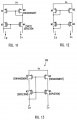
So as you can see to increase the gain replace M6 and M7 with cascode current mirror.
 

Jony130

Joined Feb 17, 2009
5,601
Here is some cascode current mirror topologies I found. Which one should I use?
I don't know, try them all in simulation.
Also don't forget that I'm not a IC CMOS designer (I'm not even a EE).
And I'm not interested to go into this subject. So I don't help you with choosing the right W/L.

Also, could you tell me how to replace M6 and M7 by cascode current mirror?
Simply delete M6 and M7 from the circuit. And place current mirror from fig12 for example.
 

Thread Starter

anhnha

Joined Apr 19, 2012
904
Thank you.

I don't know, try them all in simulation.
Also don't forget that I'm not a IC CMOS designer (I'm not even a EE).
And I'm not interested to go into this subject. So I don't help you with choosing the right W/L.
Ha, I knew that. :)
However, you know much more than I do. And I need your help in understanding circuits in general.

Simply delete M6 and M7 from the circuit. And place current mirror from fig12 for example.
Oh, I thought if we need to replace each transistor M6 and M7 by a cascode current mirror.

I tried the circuit but I didn't sure.
I simulated figure 12 and 13 and the figure 13 gives the largest gain.
My gain increased from 40dB to 50dB now.
However, that is still not enough.
 
Top