How exactly push pull follower eliminates crossover distortion..??

Thread Starter

Himanshoo

Joined Apr 3, 2015
265
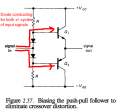
In a push pull follower to eliminate crossover distortion we bias it with diodes as shown in the figure ...
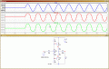
As we know that in a push pull configuration only one transistor works per input cycle...

but my query is that here since now the diodes are already forward biased via resistor R making transistor slightly 'ON' permanently... hence they would conduct for both input cycles (as shown by red arrows in 2nd figure)…now if they are conducting for both input cycles ..then how can the circuit works as a push pull follower.???????


please help
 

Attachments

ericgibbs

Joined Jan 29, 2010
18,849
hi,
The positive half cycle would drive the upper NPN harder On and the lower PNP transistor Off..
The negative half cycle would drive the lower PNP harder On and the upper NPN transistor Off.
 

Thread Starter

Himanshoo

Joined Apr 3, 2015
265
hi,
The positive half cycle would drive the upper NPN harder On and the lower PNP transistor Off..
The negative half cycle would drive the lower PNP harder On and the upper NPN transistor Off.
ok.. for positive halfcycle pnp transistor shouldn't go completely off...since it might be conducting slightly and same for negative half cycle npn transistor wouldnt be completely off...as they are biased already...

so will it be right to call them completely off...??
 

ericgibbs

Joined Jan 29, 2010
18,849
hi,
Look at the image in post #3, it shows that with no input signal [ for the first 2mSec] the current thru the transistors is approx 2.5mA.
So both transistors are 'just' conducting when there is no input signal.
See how the Off transistor current falls to zero, while the other transistor is conducting, when there is an input signal.

OK.?
E
 

Thread Starter

Himanshoo

Joined Apr 3, 2015
265
hi,
Look at the image in post #3, it shows that with no input signal [ for the first 2mSec] the current thru the transistors is approx 2.5mA.
So both transistors are 'just' conducting when there is no input signal.
See how the Off transistor current falls to zero, while the other transistor is conducting, when there is an input signal.

OK.?
E
hi,
Yes its clear in the figure what you are trying to say ...but i am wondering ..that what makes the transistor current 'off 'after 2ms..at the begining of positive input cycle...

Is it some kind of a Vbe offset (some erroneous dc signal when input voltage is zero)???
 

ericgibbs

Joined Jan 29, 2010
18,849
hi,
As you may know a silicon NPN transistor requires a Base to Emitter voltage of approx +0.65v to start conduction, a PNP transistor requires -0.65v.

The two silicon diodes are forward biased with a low current, this gives a total voltage drop of approx 1.3V, which is the same voltage level the 'paired' NPN and PNP Bases, require to just to conduct.

The 2mSec delay on my image is because I delayed the input signal by 2mS so that you could see the current when there is no input signal, is this what you are asking.?
 

Thread Starter

Himanshoo

Joined Apr 3, 2015
265
hi,
As you may know a silicon NPN transistor requires a Base to Emitter voltage of approx +0.65v to start conduction, a PNP transistor requires -0.65v.

The two silicon diodes are forward biased with a low current, this gives a total voltage drop of approx 1.3V, which is the same voltage level the 'paired' NPN and PNP Bases, require to just to conduct.

The 2mSec delay on my image is because I delayed the input signal by 2mS so that you could see the current when there is no input signal, is this what you are asking.?
no..i am asking about the output signal drop as i have marked in the figure...
 

Attachments

ericgibbs

Joined Jan 29, 2010
18,849
hi,
As I explained earlier, the polarity of the signal which drives one transistor into a higher current conduction, drives the other transistor Off.

eg: say there is no input signal, so both transistors are just conducting.

Then connect a signal source, when the positive half cycle of the signal appears at the junction of the two diodes, the Base Emitter junction voltage of the NPN is increased above the 0.65v, so the NPN collector current increases.
But the Base Emitter voltage of the PNP is reduced below -0.65v, by the positive signal, so the PNP does not conduct on the positive half cycle of the signal.

The opposite occurs on the negative half cycle of the signal.
 

AnalogKid

Joined Aug 1, 2013
11,044
but my query is that here since now the diodes are already forward biased via resistor R making transistor slightly 'ON' permanently...
Not permanently. You are correct that when the output is zero V or very low voltages, both transistors are at least partly on throughout both the positive and negative *half* cycles of the audio waveform. Let's say that because the diodes and the transistors are not perfectly matched, there is 100 mA of static current through the output transistor pair. As the amplitude of the audio increases in either the positive or negative direction, the transistors track along so there might be 1 amp going out to the speaker but there still is 100 mA going through the stack.

BUT - as the current through a transistor increases, Vbe also increases. Let's talk about your drawing in post #1 and the positive half-cycle of the audio to keep the explanation more simple. At low signal levels the Vbe's of Q1 equals the Vf of the upper diode, and the instantaneous value of signal out equals the instantaneous value of signal in. As the output current increases, Q1's Vbe increases. Now, signal out is lower than signal in by a few millivolts or tenths of volts. Q1 is supplying all of the load current from the positive power supply to the speaker, so Q2 isn't seeing any of the increased current, so its Vbe is the same low value as its diode. Because signal out is instantaneously lower than signal in, Q2's base-emitter junction is reversed-biased, and Q2 is cut off. Because of the exponential relationship between Vbe and base current, this transition is gradual, not abrupt.

This is why this type of output stage is called class AB - it is class A at low signal levels where the output current to the speaker is less than the static current through the output stage, and transitions to class B at higher output currents where the opposing transistor is completely cut off.

ak
 

Thread Starter

Himanshoo

Joined Apr 3, 2015
265
yup absolutely correct ...I got it ..

but since biasing voltages are dc voltages and as both transistors are conducting ..definitely there would be some DC output (not AC , like input signal) when there is no input voltage ....
am i right..
 

JWHassler

Joined Sep 25, 2013
306
yup absolutely correct ...I got it ..

but since biasing voltages are dc voltages and as both transistors are conducting ..definitely there would be some DC output (not AC , like input signal) when there is no input voltage ....
am i right..
The junction of R4/R5 will be at V2/2. But C2 removes this DC-component.
 

ericgibbs

Joined Jan 29, 2010
18,849
but since biasing voltages are dc voltages and as both transistors are conducting ..definitely there would be some DC output (not AC , like input signal) when there is no input voltage ....
If the push pull stage is powered from a single supply supply, say +12V, then without any input signal the junction of the two transistors would be at 12v/2 =6v.
Some push pulls are powered by dual supplies, say +/-12V, so ideally the junction of Vout would be 0v.

As JW has stated, for a single supply, a DC blocking capacitor is required between the output and the Load,in order to remove the Vsup/2 standing voltage.
 
Top