How do phototransistors work?

Thread Starter

ilium007

Joined Aug 24, 2013
139
I'm a bit confused with how phototransistors work. Q1 in the image below looks like an NPN transistor. I'm not sure why there is a positive voltage on the collector. I know it must be right because this is how I see all of these optocouplers being used but I don't understand how its working. I'm used to the NPN transistor switching the negative load.
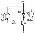
1601809225922.png
 

OBW0549

Joined Mar 2, 2015
3,566
I'm a bit confused with how phototransistors work. Q1 in the image below looks like an NPN transistor. I'm not sure why there is a positive voltage on the collector. I know it must be right because this is how I see all of these optocouplers being used but I don't understand how its working. I'm used to the NPN transistor switching the negative load.
Your diagram is (or certainly ought to be) self-explanatory: when light impinges on Q1 it conducts. This allows current to flow from Vcc down through Q1 and Rb into the base of Q2, turning Q2 on and allowing current to flow from Vcc down through the load (a relay, in this case) and through Q2 to ground.

The only real difference between your two diagrams is that the first one includes an extra stage of current amplification (Q2) to drive a higher-current load than what Q1 could handle all by itself. That is the only difference.
 

Thread Starter

ilium007

Joined Aug 24, 2013
139
I can see and understand how the circuit in the first image is working, but I am confused with NPN vs PNP internals. Q1 is an NPN device, I thought NPN could only switch a negative load?
 

Thread Starter

ilium007

Joined Aug 24, 2013
139
How can I use an emitter / collector type optoisolator to trigger a 7N2002 NPN MOSFET (I have a heap of them)
 

MrChips

Joined Oct 2, 2009
30,824
Low-side (A) or High-side (B) switch

1601815719076.png

Transistors used as current switches can be placed on the "low side" or "high side" between the power rails and the load.
This can be applied to both NPN and PNP BJTs as well as N-channel and P-channel MOSFETs.
What will change is the logic level required to perform the desired action depending on the polarity of the transistor.

Particular attention must be placed on the required turn-on and turn-off voltages in all cases.
 

atferrari

Joined Jan 6, 2004
4,771
I can see and understand how the circuit in the first image is working, but I am confused with NPN vs PNP internals. Q1 is an NPN device, I thought NPN could only switch a negative load?
Your pre-concept might be simply wrong or not suitable or...

By the time you got an explanation that seems to work and to what, at least for now, you have no argument to opose to it, you should stop trying to fit your previous idea and be ready to incorporated the recent one.
In such a simple circuit it is quite evident BTW.

Much like discarding old cloths. If there is a reason, just do it.
 
Last edited:

Papabravo

Joined Feb 24, 2006
21,228
I can see and understand how the circuit in the first image is working, but I am confused with NPN vs PNP internals. Q1 is an NPN device, I thought NPN could only switch a negative load?
An NPN device can be placed in any of three different configurations called Common Emitter, Common Base, and Common Collector (aka Emitter Follower). Nowhere is it written that an NPN device, used as a switch, can only be used with a load connected to a negative potential. Potentials are all relative anyway. Q1 is wired in the Common Collector (aka Emitter Follower) configuration, and violates no know laws of Physics or reality.
 
Top