how can i reverse engineer the schematics of this simple computer mouse

Thread Starter

Adel Beitvashahi

Joined Jun 30, 2017
5
hey i'm new to electronics and i'm working on making a drawing pen out of this mouse so I need to desolder all the parts out of the pcb and put them together in a way so that they can fit in a relatively thin pen for drawing, my problem is i dont know how each part is connected, i have looked online and couldnt find a schematic for the mouse product. its a mini ihome mouse

are the dark green lines wire connections or the light green parts?
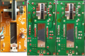
here are some pics

yellow - Copy.jpg green - Copy.jpg
 

WBahn

Joined Mar 31, 2012
29,930
The light green is the copper. Consider that the copper has to connect the pins that are soldered into the board, so the regions surrounding each pin have to be copper.

I suspect you'll find getting it into a workable pen is going to be much easier said than done, but good luck.
 
Crash course:
A single sided when it's made has a bunch of holes and a silk screen (part designations) on the top layer.
The bottom layer at one point was solid copper. A UV resist was applied, developed and exposed and the copper etched.

You were left with tracks and exposed copper areas. Making the board mostly copper is less wastefull.
SOLDER resist is applied which is usually green that covers the entire PCB except the pads.
So, your seeing the contrast of the board and copper traces.

One processes used for the pads (where components are soldered) is HASL. This is where a layer of solder is applied at leveled with hot air, hence Hot Air Level Solder.

Now, the board can be drilled.

This is just a quick overview for the board I see. A single sided PCB. it gets a lot more complicated.
 

Dodgydave

Joined Jun 22, 2012
11,277
Looks like you have removed the 8 pin dil chip and 4 pin lens, you can see the Sda and Slc wires to the usb, the other two are +/-5v, the other 4pins on the chip will be for left right buttons and up/down wheel clocking,.. So you're best solution is to look for mouse circuits using the same chip number.
 
Last edited:

atferrari

Joined Jan 6, 2004
4,763
The visual recognition is of help, BUT and it is an important but, measuring continuity is the way to identify connections with not even seeing the actual copper trace.

My suggestion: Identify always first the common rail. Then the power rail.

Once there, go to connectors and try to identify whatever could be considered input or output.

Use in the beginning a huge sheet of paper where your schematic mimics the physical layout of the actual PCB.

Once you think you are done, check the circuit with power on. Be aware that the circuit could be out of order.

Buena suerte.
 

Thread Starter

Adel Beitvashahi

Joined Jun 30, 2017
5
so since its a single sided pcb, can i assume that everything on the same block of light green (copper block) is to be connected to each other in no specific order?
 

Thread Starter

Adel Beitvashahi

Joined Jun 30, 2017
5
thank you everyone for the answers. I just went over the pictures and drew some links between the pins which were in the same copper block.
gonna crop the parts out and connect their pins to make it like a proper schematic and test it on breadboard
 

Thread Starter

Adel Beitvashahi

Joined Jun 30, 2017
5
busy week. just took out all the parts and soldered some wires to them so i can mount them on breadboard.

here is what i thought were the connected parts and the other two pics for reference. (the pic on the left is horizontally flipped btw, so originally the green switch is on the left side)
upload_2017-7-7_12-53-36.png

two questions:
the two cyan pins in the middle picture are from the mouse switches and it looks like they are connected to nothing, does that mean they are grounded?
i'm trying to connect all the parts on the breadboard but i'm not sure how to connect those two to ground, can i just connect them to nothing and call it a day?
thank you very much for helping me!
 

Attachments

Top