How can gate driver's power side be connected if the inverter topology is not a half bridge based?

Thread Starter

BrokenPin

Joined Oct 1, 2023
21
Hello all,

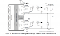
I am trying to build a hardware setup for a PEC9 inverter. Since it has more switches and a different configuration than a regular half/full bridge (meaning no high and low side), I didn't know how to connect the gate driver's power side pins (VDD/VSS) since usually in a half-bridge topology the source of the high side switch connects to the drain of the lower side switch and the VEE of the upper gate channel (like in the attached image) and also the VSS of the bottom gate channel is connected to the lower side switch source.
How can I connect the VSS of both gate driver channels to the MOSFETs in the PEC9 topology? Or can I leave them unconnected to the MOSFETs as they are used to power the gate driver's power side?
I will be using 4 dual-channel gate drivers to drive all the MOSFETs or switch to single-channel ones but will still use an isolated bipolar bias supply for each gate driver.

2-Figure1-1.pngbipolar gate drived.png

Regards,
 

Attachments

ronsimpson

Joined Oct 7, 2019
3,248
Top side Gate drivers with "Rboost & Diode" do not work well in inverters. You must understand how they work or don't use them.

Because I don't remember how PEC9 works, I would use single Isolated Gate drivers IC with isolated power supplies for each IGBT. You will need a separate isolated power supply for each IC. There are many 8-pin isolated gate driver ICs in the market.
1719241408324.png
Here is an example of a DC to DC power supply with 3000V of isolation. I am using a 12V to 12V version but there are 15:15, 5:12, and many others.
1719241227964.png
-----------I have revisited the problem------------------
There are a number of cases where there are a pair of IGBTs with common Emitters. I redrew the circuit moving S5 so it is easy to see how a dual gate driver could work. You will need a floating power supply that connects at "negative supply4-5" and "Pos supply4-5". A pair of isolated Gate drivers, or a dual isolated Gate driver will control S4 & S5.

Do you drive S4 and S5 with the same signal?
1719242138624.png
Also, S7 looks strange. I think both transistor will brake. I believe this is a simplified drawing with pieces missing.
------------edited-------------
This circuit is slightly different. I don't know why.
Note S7, the Gates cannot be tied together. They need the same signal. Use two different Gate drivers!
1719244125938.png
 
Last edited:

Thread Starter

BrokenPin

Joined Oct 1, 2023
21
Thank you @ronsimpson for the detailed answer.
I would use single Isolated Gate drivers IC with isolated power supplies for each IGBT. You will need a separate isolated power supply for each IC. There are many 8-pin isolated gate driver ICs in the market.
Understood, I will use a single-channel gate driver instead of a dual-channel. I already designed a +15V/-4V isolated bias supply for each switch gate driver.
There are a number of cases where there are a pair of IGBTs with common Emitters.
There are only S4 and S5 that have their emitters meet at a single point, which can be driven by a dual-channel gate driver. the others need to have separate single-channel gate drivers with isolated bias supply, right?
What I am not sure about is, whether should i connect the negative bias (VSS) to the emitter/source of each switching device or not since in this topology switches aren't in pairs like in the case of half-bridge (circled in red and blue in attached image).
Or should I just connect the positive and negative bias of the isolated power supply (+15V/-4V) to the gate driver's VDD and VSS pins and connect only the gate of the switching device to the gate driver's OUT pin!!?


Note S7, the Gates cannot be tied together. They need the same signal. Use two different Gate drivers!
Thank you, I was about to make a huge mistake by tying them together and using only one signal.
 

ronsimpson

Joined Oct 7, 2019
3,248
Isolated Power Link to a data sheet. I was looking for this part: VQA3S-S15-D15-S
Digikey +15V & -4V Here is a list of isolated power, I was looking for +15V and -4 or -3V out.
I connect the IC from +15V to -4V. Connect the Emitter to 0V of the isolated supply. (add caps from 15 to 0, -4 to 0 and 14 to -4)
This way when the Gate is on, there is about +15V G-E and when the Gare is off there is about -4V G-E.
I have used other ways but this is simple.
Because the +15/-4 is hard to get you might use a +/-15V supply and add a LM79L05 to make -5V. The average current in the supply is not very much. The peak current might be 5A but the average is almost zero.
 

MrAl

Joined Jun 17, 2014
11,755
I will send it to you once I finish the design.

Hello there,

What was being discussed here sounds good to me too. When we did converters we used an isolated power source for each driver for each transistor, no matter how many transistors were involved. For bipolars that means the emitter went to ground of that power source, and that's the main issue, and that the leads had to be as short as possible, and also with at least some kind of snubber for each and every transistor. For Mosfets lead length is even more important because switching speed is usually a big concern, as well as keeping local oscillations as damped as possible.

If you are still unsure of how this is going to work, just do a simulation and check the voltage for each and every transistor terminal (for bipolar that would be emitter, base, and collector) and also the current. That will tell you if you are driving them correctly.
You also have to check for voltage spikes across each transistor (bipolar would mean collector to emitter) and that tells you if the transistor might blow out due to an overvoltage. Of course the driver has to supply whatever input current is needed for whatever transistor type you intend to use. Mosfets at least 1 amp.
The most important wiring is to the emitter or source. It should be short.
Also, each driver must have adequate bypass capacitor(s) so that the driver has a very local current source available. It does not help to use a 2 amp driver it the driver can not actually get 2 amps for a short time anyway, and all sources have some series inductance which is always a consideration for high current drivers (even 1 or 2 amps would be considered high in this application).

If a PC board, the driver traces should be wide to reduce inductance.

Just a few extra notes here.
 
Last edited:
Top