Facebook
 Google
 GitHub
 Linkedin
eetech00 - I have studied your very detailed explanation and have a couple of questions.
1) For the pMOS, you write -20V, 2A. Does this mean Vdss should me a "minimum" of 20V, so you don't fry the pMOS?
2) Also for the pMOS, does the 2A simply mean that it needs to be able to handle "maximum" of 2A?
3) FQU17P06 is about $0.40 from Newark (such a deal!). It has Vdss -60V, and Id -12A. Does that meet the criteria, and am I reading the spec correctly? There are so many parameters listed on the cut sheet - it is hard to decipher all of the information and what is relevant to the design.
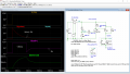
As C1 continues to charge up, the voltage at the base of Q1 gradually decreases at a rate determined by [R1|R2R3]C1.
4) Is the terminology/theory here called a "bridge"?
5) Why use 3 resistors, and how do you decide on the relative resistance values of each resistor?
1) For the pMOS, you write -20V, 2A. Does this mean Vdss should me a "minimum" of 20V, so you don't fry the pMOS?
2) Also for the pMOS, does the 2A simply mean that it needs to be able to handle "maximum" of 2A?
3) FQU17P06 is about $0.40 from Newark (such a deal!). It has Vdss -60V, and Id -12A. Does that meet the criteria, and am I reading the spec correctly? There are so many parameters listed on the cut sheet - it is hard to decipher all of the information and what is relevant to the design.
As C1 continues to charge up, the voltage at the base of Q1 gradually decreases at a rate determined by [R1|R2R3]C1.
4) Is the terminology/theory here called a "bridge"?
5) Why use 3 resistors, and how do you decide on the relative resistance values of each resistor?