High Voltage Buck Converter

Thread Starter

gdylp2004

Joined Dec 2, 2011
101
Hi guys,

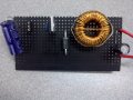
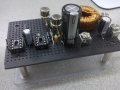
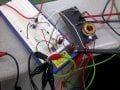
I've managed to solder the high current part of the circuit on the stripboard so that I could run it on high current (up to 3.6A DC at o/p).

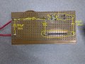
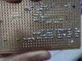
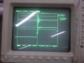
The rest of the circuit was still made on breadboard because the current rating is not high (in mA range) (see attached). Did a high current test and was happy that it is successful. However I've seen that the o/p voltage has spikes which is rather high (see attached).

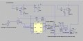
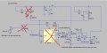
I thought I've already included a smoothing capacitor which is the 150uF capacitor (see orginal circuit in previous post), could anyone advise why there is still spikes going on?

Should I add in a RC snubber to suppress these transients?

Thank you.
 

Attachments

SgtWookie

Joined Jul 17, 2007
22,230
I didn't realize you had long wires running everywhere.

Get everything on one PCB, with the traces/interconnecting wiring as short as possible. Lay it out using a tool like Cadsoft Eagle Schematic & PCB.

Those long wires have an inductance of about 50nH per inch. It adds up really quickly, and will wreak havoc with your signals. The upper trace on your O'scope looks almost exactly like a simulation I posted a few days ago regarding parasitic inductance and capacitance, and how to snub it.

Good luck with your layout. I'm in the hospital, and am going into surgery in a couple of hours for heart bypass. I'll be offline for at least three days, and won't have access to tools like Cadsoft Eagle nor LTSpice (not even MS Paint) for probably a couple of weeks or more.
 

Thread Starter

gdylp2004

Joined Dec 2, 2011
101
I didn't realize you had long wires running everywhere.

Get everything on one PCB, with the traces/interconnecting wiring as short as possible. Lay it out using a tool like Cadsoft Eagle Schematic & PCB.

Those long wires have an inductance of about 50nH per inch. It adds up really quickly, and will wreak havoc with your signals. The upper trace on your O'scope looks almost exactly like a simulation I posted a few days ago regarding parasitic inductance and capacitance, and how to snub it.

Good luck with your layout. I'm in the hospital, and am going into surgery in a couple of hours for heart bypass. I'll be offline for at least three days, and won't have access to tools like Cadsoft Eagle nor LTSpice (not even MS Paint) for probably a couple of weeks or more.
Wish you well in your surgery and a speedy recovery.
 

Thread Starter

gdylp2004

Joined Dec 2, 2011
101
Hi guys,

Does anyone know how to simulate a voltage "ringing" in LTspice for the Buck circuit I've built earlier.

The prob is the real circuit does have transient but the simulation do not. What should I tweak in the schematic in LTspice to simulate that "ringing"?

I think I've understood abit on how to tackle the transient prob by adding a RC snubber across the drain-source terminal of the power MOSFET but would like to try it in simulation first.

Anyone has any clue?
 

SgtWookie

Joined Jul 17, 2007
22,230
Just add inductors in series with the interconnecting traces. Instead of just Ln, give them a reference designator like LPARn to differentiate it from a standard inductor.

TO-220 package leads have about 7nH inductance each.

Give the other parasitic inductors a value of 50nH per inch. It actually varies for wire diameter, etc. - but it will be plenty close enough for a simulation.

If the interconnecting node is a ground or power plane on a multilayer circuit board, it won't have any inductance.

Breadboards have lots of parasitic inductance and capacitance. You would have to measure your particular board to find out what it is.
 

Thread Starter

gdylp2004

Joined Dec 2, 2011
101
Just add inductors in series with the interconnecting traces. Instead of just Ln, give them a reference designator like LPARn to differentiate it from a standard inductor.

TO-220 package leads have about 7nH inductance each.

Give the other parasitic inductors a value of 50nH per inch. It actually varies for wire diameter, etc. - but it will be plenty close enough for a simulation.

If the interconnecting node is a ground or power plane on a multilayer circuit board, it won't have any inductance.

Breadboards have lots of parasitic inductance and capacitance. You would have to measure your particular board to find out what it is.
Thank you! Hope you're doing well.
 

Thread Starter

gdylp2004

Joined Dec 2, 2011
101
Hello everyone,

I've changed my IRF640NPbF nMOS into IRFB4227PbF and adding a 200V 100uF bypass cap decoupling the +HV 100V (see attached schematic).

Upon turning on my HV 100V PSU, the stripboard suddenly smokes and an awful smell is given off. Went to check what's wrong and realised there is an interesting distinct path that was burnt (see buck_on_stripboard_back.jpg). The components facing side photo is also uploaded (see buck_on_stripboard_face.jpg).

From my guess, when I've turned on the 100V PSU, a surge travels down starting from the MOSFET's drain, 100uF supply bypass cap, schottky (FW) diode and to somewhere else.

The schottky diode was found to be damaged. The burnt marked also ends at the anode of the schottky. But what I did not understand is why didn't the current continue to flow pass the anode of the FW diode and all way to GND, but instead through the diode.
 

Attachments

Thread Starter

gdylp2004

Joined Dec 2, 2011
101
HI guys,

Im back. I've put everything on a board.

When I turned on the 100V PSU, by slowly ramping up the DC voltage starting from 0V, only 2 out of 10 times will produce the expected result. The other 8 times, either they have no response, as in no o/p voltage or the drain and source got short together, destroying the MOSFET.

Does anyone knows why? I've appended my circuit, PCB layout diagram, as well as the actual photo. Basically, everything.

Any comments are welcomed.
 

Attachments

SgtWookie

Joined Jul 17, 2007
22,230
Your MOSFET is getting smoked at turn-on.

You need to soft-start your PWM input. Otherwise, the inductor saturates, which makes it seem to the MOSFET that it has your 100v supply directly across it until the cap charges.

I am still in the hospital, but moving towards discharge. I do not know if I will have Internet access for the next few weeks..
 

Thread Starter

gdylp2004

Joined Dec 2, 2011
101
Your MOSFET is getting smoked at turn-on.

You need to soft-start your PWM input. Otherwise, the inductor saturates, which makes it seem to the MOSFET that it has your 100v supply directly across it until the cap charges.

I am still in the hospital, but moving towards discharge. I do not know if I will have Internet access for the next few weeks..
I am currently using a Function Gen to produce the PWM and how could I soft start it? Do I set initial duty cycle = 0%, turn on HV PSU and slowly ramp from 0-100V, then lastly, ramping duty cycle from 0%-28%? Is this OK?
 

Thread Starter

gdylp2004

Joined Dec 2, 2011
101
Yes, that should help a great deal.

Later, you can work on automating the adjustment.
I think I've to do these steps fast, as you can see from my schematic that the 2 IC DIP8 chips are powered by 2 different series linear regulator from the 100V and 28V respectively. What I am concern is if I do not switch the PWM to 28% fast enough, the control's circuit will be powered by the 100V series linear reg instead of the 28V's because basically, there is no o/p voltage. Only once after I've ramped close to 28V, the current drawn would then be switched over to the 2nd series reg (28V's) which is the one to expect to turn on for a steady state operation because of its relatively lower power dissipation.

I've tried only allow the 100V's series reg to supply the IC chips but the power dissipation is too great for the BJT to handle, hence burnt and destroyed. This is also the reason why I add another similar one at the 28V's o/p.
 

Thread Starter

gdylp2004

Joined Dec 2, 2011
101
Hi SgtWookie,

I tried soft starting PWM by increasing the duty cycle % in steps of 5% but to no avail.

To troubleshoot, I've changed the MOSFET, two NPN transistors and ALL of the zener diodes. In fact, those zeners are still functioning after I've removed them out of the stripboard.

Next, I also connect the control circuit (inclu. IR2117, TC4420EPA, Cbst, Rbst, Dbst all on breadboard to check if the HV side of the circuit is working properly. The test results in the end proved OK.

I really have changed all those components that I think might have spoilt but it still doesnt work, including soft starting it as you suggest.

I've then try to attempt to troubleshoot in a more detailed way by setting V+ = 10V, 30V and observe the base of the NPN transistor (100V linear series reg.) and realised that the base voltage (or the zener voltage) did not have the chance to climb till 12V. In theory, as long as V+ > 12V, the 12V zener will hold at this voltage even if we ramp more than 12V to V+.

But according to the both graphs attached, (one @ V+ = 10V, one @ V+ = 30V), the latter should already have a high enough voltage to ramp Vb > 12V? But the waveform on oscope doesnt seems to be the case (see 2nd attachment).

The waveform tells me that Vb attempts to rise but dropped to zero immediately after ~3.2V like that.

WHY? This could be the very reason why my circuit cant work because the IC doesnt have a 12V Vdd to start with.
 

Attachments

Thread Starter

gdylp2004

Joined Dec 2, 2011
101
I've changed the NPN trnasistors to 2N5682 and 2N5600 but still the same.

Anyone knows why? Could it be the zener I'm using is not suitable?

Or I should increase the base resistor?
 

Thread Starter

gdylp2004

Joined Dec 2, 2011
101
Hi guys! im back.

Recently I've used a 8051 MCT to control the duty cycle (%) of the PWM I fed into the system to control the gate of the nMOS. The adjustment of the PWM (increase or decrease) is actually based on the output.

Mine operating logic is simple. If output is > 28.1V, decease PWM %, and if < 27.9V, increase PWM%, otherwise PWM duty cycle = no change.

My step change is about 0.4% because I am using an 8-bit register (256 steps in total).

However here comes the problem, quite oftenly, whenever the change occurs, the circuit will suddenly goes haywire. Components highlighted in the attached circuit marked with a red cross just suddenly "blow" out, killing them instantly.

Would anyone please advise, which component should I start looking into changing them for a better rating? I've really no idea and hope anyone with great electronic experience could give me some direction or pointers to let me start instead of wasting time on others..

Thanks in advance!
 

Attachments

circuit.JPG Vgs waveform.JPG Vd w.r.t Ground.JPG
Hi guys,

I'm new in here and hope I could get some advices.

I am designing a 100V-28V DC-DC Buck converter but has encountered a problem when choosing a suitable high-frequency switch. As suggested by many designers online, pMOS is preferred for Buck operation. However one big issue is the limitation of the Vgs (typ: +-20V) which I believe is the reason why I could not utilize this as what other designers usually do.

As seen in the attached schematic, in order to turn off the pMOS switch, Vg must not be lower than both Vs and Vd by the threshold voltage indicated by the manufacturer. That is, |Vgs|< |Vth| & |Vgd| < |Vth|. Since Vs is always 100V (because source is tied to +ve terminal of battery) and Vd = 28V (assuming the capacitor is large enough to hold the charge, hence o/p voltage well) and assuming the Vth is -4V, is it correct that to turn switch off, Vg must be > Vs-|Vth| and also Vg > Vd-|Vth| since a pure MOSFET drain and source is interchangeable.

If this is true, a typical pMOS with only Vgs max of 20V could not handle since we must ramp up Vg all the way to 96V and above (for my case) but that also implies the potential difference between Vg and Vd is 68V which is > 20V and thus the FET will breakdown.

And if everything I've explained is true, is there a way to overcome this? TIA.
Vgs waveform.JPG circuit.JPG
This idea is really good and I was trying to come up with solution to avoid |Vgs| going above 20V for PMOS, without using any driver IC.
I simulated the circuit in the attached file on LTSpice. As you mentioned, I used 100V supply and still managed to limit Vgs to 0 to -10V. I used a 12V battery as a load. I am sure Vgs will not change even if its a resistive load.

Initially i thought of using resistor dividers to limit Vgs. But resistors will slow down the turning ON of MOSFET and lead to higher switching power dissipation. So i shifted to what looks like a capacitor divider (i don't if there exists such a thing) with totempole arrangement of BJTs.

Someone please verify this circuit.

Attachment:
1 - Circuit that I simulated
2 - Vgs waveform
3 - Vd waveform with respect to ground.
 
Top