High Voltage Buck Converter

Thread Starter

gdylp2004

Joined Dec 2, 2011
101
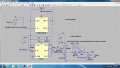
On second thought, it seems that it is inevitable that a 3.52W has to be wasted from either the Q1 or R1 if a constant 40mA is needed to sink to load and a differential voltage of 88V between HV and LV is present. There is no way I could "escape" since this 40mA has to pass through this 88V no matter what, hence constitute the 88X0.04=3.52W wastage.

And the so called better efficiency is for shunt regulator, when the load is off (disconnected), the full 40mA has to be dumped to the Zener diode as useless energy. But for the series method, when the load is switched off (or gradually lightened, the power dissipated by the NPN would reduce as well since current through CE is actually nothing but the load current, while assuming negligible base current.
 

SgtWookie

Joined Jul 17, 2007
22,230
I don't know how you came up with 40mA?

You were saying earlier that it was around 7.1mA.

I modified an earlier version of your circuit so that all of the 15v supply current was flowing through a 1-Ohm sense resistor, and reading the voltage across that via a low pass filter. See the attached.

R3 was selected to allow 20mA current to pass across 85v. It should have a 3W power rating.
The Zener has been changed to 15v. The IR2117 has a voltage range of 10v to 20v; if the input voltage is outside of that range, the IC will shut down. To keep it in the operating region, I selected 15v as the midpoint. I was trying to infer this to you earlier, but you kept repeating 10v.

Earlier in your shunt regulator, you were not using a capacitor at the output. I tried to imply this by getting you to think about what the difference was between an ideal voltage supply and an ideal current supply.

An ideal voltage supply has zero impedance, and an ideal current supply has infinite impedance. Having a large resistor across 85V-90V is a pretty high impedance source of current if you ask me.

You can change that from a high impedance source to a low impedance source by adding a capacitor. I was trying to get you to refer back to where I told you that Cbias needs to be 10x the size of Cbst. You appear to have completely forgotten about that, and it has cost you a great deal of flailing around.

I reduced Cbst to 1uF, increased Cbias to 10uF, and there is also C1 at 10uF the other side of Rsense. I have the simulation start with those three caps charged to 14v to speed the simulation up. Note that Cout is back up to 150uF.

You still have problems with overshoot, and there is no regulation on the output voltage, as there is no feedback.
 

Attachments

Thread Starter

gdylp2004

Joined Dec 2, 2011
101
Hi wookie,

I've realised the 7.1mA was actually the avg current for the optocoupler instead of the IR2117 gate driver. I, myself got a little confuse thus I quickly went to lab and get the new readings which turns out to be 40mA.

Also, although the datasheet says the range of Vcc is 10-20V, through experimental trials, it turns out the lower limit is about 9.6V before it turns off IR2117, and the upper limit is about 16.6V before it starts attenuate my duty cycle unwillingly. So in view of this, I have also changed the Vcc into 12V and clipping V(gs) that voltage as well. Somewhere between 9-16V. And the initial reason why I insisted on 10V was because before the use of differential probe, I had seen over voltage (>20V) going across gate-source, and hence I set to a low 10V for protecting the nMOS. After using differential probe, there was no overshoot actually.

Regarding the impedance topic, I think I need more time to digest.
 

Thread Starter

gdylp2004

Joined Dec 2, 2011
101
I tried to calculate Cbst again using the formula found in page 6 of http://www.irf.com/technical-info/appnotes/an-978.pdf.

Qg=60nC by assuming V(ds) = 100V. Not sure if this is a good estimate as the graph indicates I(d) =11A which is quite different from mine.

f=100kHz

Icbs(leak)=0.5μA By referring to since CR=1μF X 0.008 X UR=25V = 0.2μA which is < 0.5μA datasheet: http://www.farnell.com/datasheets/438266.pdf


Iqbs(max)=240μA obtained from IR2117 datasheet: http://www.irf.com/product-info/datasheets/data/ir2117.pdf

Vcc=15V

Vf=0.875V from MUR120 datasheet: http://www.farnell.com/datasheets/92109.pdf


Vls=-0.85V from STPS3150 datasheet: http://www.st.com/internet/com/TECHNICAL_RESOURCES/TECHNICAL_LITERATURE/DATASHEET/CD00003323.pdf

Vbs(min)=10V from IR2117 datasheet


Qls=5nC as recommended by the IRF boostrap guide

Finally, calculated Cbst=~51nC

If my individual values are correctly assumed, then it seems that a 10uF I've used earlier could be an overkill as it definitely lengthen the initial charging period of Cbst?
 
Last edited:

SgtWookie

Joined Jul 17, 2007
22,230
Not only overkill; you most likely had a much higher ESR with a larger cap than if you'd used a smaller one.

You also were not using a Cbias that was 10x the value of Cbst.

The initial charge time for Cbst isn't such a big deal, unless you need a really fast turn-on time for the supply. The IR2117 should keep itself disabled until the voltage comes up.

I don't have a model for your HCPL-3180 optocoupled driver. I'd looked for them before, but Avago had not published any at that time.

They DO have models published for the -3120 and -3140:
http://www.avagotech.com/pages/optocouplers_plastic/spicemodels/
You could go ahead and evaluate the datasheets between them and the -3180 to see which would be more representative, and then request a copy of the SPICE macro.
 
Last edited:

Thread Starter

gdylp2004

Joined Dec 2, 2011
101
Not only overkill; you most likely had a much higher ESR with a larger cap than if you'd used a smaller one.

You also were not using a Cbias that was 10x the value of Cbst.

The initial charge time for Cbst isn't such a big deal, unless you need a really fast turn-on time for the supply. The IR2117 should keep itself disabled until the voltage comes up.

I don't have a model for your HCPL-3180 optocoupled driver. I'd looked for them before, but Avago had not published any at that time.

They DO have models published for the -3120 and -3140:
http://www.avagotech.com/pages/optocouplers_plastic/spicemodels/
You could go ahead and evaluate the datasheets between them and the -3180 to see which would be more representative, and then request a copy of the SPICE macro.

Ok, I start to see why you keep re-emphazing that I was not using a Cbias that is 10x than Cbst although I already did change my Cbias to 150uF immediately once you've highlighted this necessary move in post #44.


It was the 10uF that I've parallel it with the Zener diode which has falsely portray that I've not learned about the 10x requirement. My apologies as the 10uF I've added was purely a ball park figure for me to observe what's the difference after I've added a decoupling capacitor.


I would change the value to 100uF or more if I had integrate this shunt linear regulator with the IR2117.


Also, if you were to ask me, the bypass capacitors (aka decoupling caps) are capacitance connected in parallel to protect against acceptable transient occuring at the point-of-interest by compensating any loss of charge, hence voltage for a very short period of time. The duration that the capacitor can hold the charge (or voltage) really depends on the capacitance value. Under extreme cases, when the capacitance is so high, the capacitor is actually nothing but a battery.


I am not sure if this logic is the same as what you try to infer to be about the differences between an ideal voltage or current supply impedances.

If it is not, I would be more glad to read up more.
 

SgtWookie

Joined Jul 17, 2007
22,230
It's important that you keep your schematic representative of your existing circuit, as close as possible, when you post it. If there are large differences and you don't show them, particularly if I've suggested a change and you don't show the change, then I will have to assume that you did not implement the suggestion and I will waste time wondering why not.

It's also important to document lengths of connections; if you have wire runs that are more than a couple of inches long, their parasitic inductance can wreak havoc with circuit performance. Even straight wire has inductance, and it adds up pretty quickly.

A straight piece of 1mm diameter (AWG-18) wire that is 1" long has about 25nH of inductance. The inductance goes up if there are bends/kinks in the wire.
 

Thread Starter

gdylp2004

Joined Dec 2, 2011
101
Ok, got it.

Does anyone knows how could I interface my Schottky diode into one of the holes in my stripboard?


The diameter of the lead of the Schottky is about 1.3mm, which is 0.3mm wider than the 1.0mm hole in the stripboard. I intend to drill a 1.5mm hole right in the middle since the pitch (trace width of the stripboard) is about 2.54mm, which still has enough copper for me to solder later on.

Or is there any connector I can buy to fit the thick 1.3mm lead into and then fit everything to the 1.0mm hole. But this introduce alot of parasitic elements like contact resistance and etc?

Schottky diode datasheet for your convenience: http://www.st.com/internet/com/TECHNICAL_RESOURCES/TECHNICAL_LITERATURE/DATASHEET/CD00003323.pdf
 

SgtWookie

Joined Jul 17, 2007
22,230
If you must, just strip a short piece of 1mm wire, wrap it around the diode's lead a few times, solder it, and stick the end through the hole.

But, if you use a pair of diagonal cutters and snip the end off at an angle, the end will be pretty sharp and you could use that to drill into the board.
 

billbehen

Joined May 10, 2006
39
You are worying too much! Vd, the drain voltage will never be 28 Volts DC. Due to the inductor, Vd will either be just under 100Volts when the switch is turned ON, and will be about GND when the power diode is ON and the FET is OFF.

All you have to do is get Vg, the gate voltage down to 85 Volts or so to turn the FET ON, then "let go of it" and let it drain thru a gate - source resistor. A zener from gate to source is not a bad idea, as suggested above, etc.
 

SgtWookie

Joined Jul 17, 2007
22,230
You are worying too much! Vd, the drain voltage will never be 28 Volts DC. Due to the inductor, Vd will either be just under 100Volts when the switch is turned ON, and will be about GND when the power diode is ON and the FET is OFF.
I can only guess that you are commenting on something very early on in the thread; this post will make it 8 pages long.

You really need to quote the post you are responding to.

All you have to do is get Vg, the gate voltage down to 85 Volts or so to turn the FET ON
This is quite incorrect.
You must always refer to Vg as Vgs, rather than VgGND. If you try to think of the gate voltage relative to GND instead of the source terminal, you will wind up with a big pile of blown MOSFETs.

...then "let go of it" and let it drain thru a gate - source resistor.
This is also not correct.
In this application, it is actually OK for the MOSFET to have a somewhat slow turn-ON time; as if the inductor is being operated in discontinuous mode (as it should) then when the MOSFET first turns ON, the current will be zero, and will take time to increase.

However, the turn-OFF needs to be pretty quick, or the power dissipation in the MOSFET will be huge. I believe I demonstrated that; I posted a modification of the proposed circuit's gate drive which reduced power dissipation in the MOSFET by well over 90%.
 

Thread Starter

gdylp2004

Joined Dec 2, 2011
101
However, the turn-OFF needs to be pretty quick, or the power dissipation in the MOSFET will be huge. I believe I demonstrated that; I posted a modification of the proposed circuit's gate drive which reduced power dissipation in the MOSFET by well over 90%.
I remember that, it is a diode connected in anti-parallel with the gate resistor to provide a faster discharge time by giving the current flow an alternative.
 

Thread Starter

gdylp2004

Joined Dec 2, 2011
101
I think I'm in deep trouble now as I've unknowingly killed 3 IC chips at one go after I've changed the Cbias from a 150uF electrolytic cap to a 10uF tantalum cap.

The first damaged chip was easily identified when a small spark sound upon turning on my 12V DC supply to the IR2117 gate driver. I happen to catch a glimpse on the digital reading of the DC PSU (about an overshoot of 35V or more, then quickly back to 12V). After that, the chip has a burnt smell too and I know it is already a goner.

While not aware of the cause of the problem, I've later found out that the another IR2117 chip as replacement has also turned faulty (but this time a silent killer) and another TC4420 chip was also not functioning properly (although I did test it is working earlier).

I would like to know if the 10uF tantalum cap is the culprit as mainly because, lets take the IR2117 driver for example, has absolute no problem no matter how many times I had turn on the 12V DC power supply with a 150uF electrolytic cap.

Could it be the reduction of the capacitance value or the type of the cap that is killing my IC one by one. Or is it both?

Please note that my Cbst has been changed to 1uF this morning and thus 10uF, is still 10x more than Cbst.

Why is it like this? I do not wish to damage anymore ICs as ordering these components could take 5 working days. :(
 

SgtWookie

Joined Jul 17, 2007
22,230
Tantalum capacitors can be problematic. They usually have a very low ESR, but are intolerant of overvoltages; they'll blow immediately. They are also particular about how long they have been sitting around idle; if you suddenly apply power to a tantalum cap that's been sitting around for even just a few months, it can pop with a bang, taking out several components nearby.

You will likely be better served by using low-ESR aluminum electrolytic capacitors, or several caps in parallel. Using multiple smaller caps in parallel lowers the equivalent ESR.
 

Thread Starter

gdylp2004

Joined Dec 2, 2011
101
Tantalum capacitors can be problematic. They usually have a very low ESR, but are intolerant of overvoltages; they'll blow immediately. They are also particular about how long they have been sitting around idle; if you suddenly apply power to a tantalum cap that's been sitting around for even just a few months, it can pop with a bang, taking out several components nearby.

You will likely be better served by using low-ESR aluminum electrolytic capacitors, or several caps in parallel. Using multiple smaller caps in parallel lowers the equivalent ESR.
Thanks, so could we rule out that the reduction of the capacitance value most probably won't cause the IC to fail abruptly?
 

Thread Starter

gdylp2004

Joined Dec 2, 2011
101
Did you change any other parts when you changed the 150uF aluminum electrolytic for the 10uF tantalum cap?
Yes, I've replaced the 10uF Tantalum Cbst with a 1uF also tantalum Cbst. And changed the 150uF electolytic cap into 10uF tantalum cap since Cbst is 1uF now therefore Cbias could be reduced.

I had also interfaced TC4420 chip with IR2117 with also a 10uF tantalum cap biasing the TC4420 chip as well. The TC4420 is basically to convert the PWM of 3.3V peak to a 12V peak because IR2117 doesn't allow 3.3V as Vin (min is about 7V peak).

I did my first test it was running perfectly and succeeded in switching my nMOS at the end, but the second try fails.

I went to debug and realised that as long as the PWM input signal touches the Vin pin of IR2117, the signal collapsed, while for the TC4420, if the PWM touches the Vin pin, the PWM signal rises to the mean of its value. Basically this is not right. Went to do a continuity check on Vin pin if it is shorted to GND, but it isn't.
 

Thread Starter

gdylp2004

Joined Dec 2, 2011
101
Yes, I've replaced the 10uF Tantalum Cbst with a 1uF also tantalum Cbst. And changed the 150uF electolytic cap into 10uF tantalum cap since Cbst is 1uF now therefore Cbias could be reduced.

I had also interfaced TC4420 chip with IR2117 with also a 10uF tantalum cap biasing the TC4420 chip as well. The TC4420 is basically to convert the PWM of 3.3V peak to a 12V peak because IR2117 doesn't allow 3.3V as Vin (min is about 7V peak).

I did my first test it was running perfectly and succeeded in switching my nMOS at the end, but the second try fails.

I went to debug and realised that as long as the PWM input signal touches the Vin pin of IR2117, the signal collapsed, while for the TC4420, if the PWM touches the Vin pin, the PWM signal rises to the mean of its value. Basically this is not right. Went to do a continuity check on Vin pin if it is shorted to GND, but it isn't.
BUMP. 10char.
 

SgtWookie

Joined Jul 17, 2007
22,230
I'm rapidly losing interest in your project, as you consistently omit details that can be critical.

I don't see schematics to demonstrate your various configurations, and O'scope shots to show the waveforms.

If I can go to the trouble of generating multiple schematics for many online members, surely you can at least provide accurate and complete schematics of YOUR circuit to show exactly how you have it configured.

Otherwise, I have to start guessing, and guessing is quite often wrong.
 

Thread Starter

gdylp2004

Joined Dec 2, 2011
101
I'm rapidly losing interest in your project, as you consistently omit details that can be critical.

I don't see schematics to demonstrate your various configurations, and O'scope shots to show the waveforms.

If I can go to the trouble of generating multiple schematics for many online members, surely you can at least provide accurate and complete schematics of YOUR circuit to show exactly how you have it configured.

Otherwise, I have to start guessing, and guessing is quite often wrong.
Ok, attached is the complete schematic that represents my actual circuit now. Not sure, if this is good enough to attract back your interest, as you are the ONLY one who has been consistently replying my thread in this forum.

Do let me know if you need other information.

Happy new year to everyone!
 

Attachments

Last edited:
Top