Facebook
 Google
 GitHub
 Linkedin
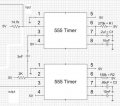
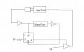
Cheers everyone. I designed the attached circuit but it is not quite doing what I wat it to do. It works like this:
The clock drives this logic circuit that passes through a tri state buffer. This tri state buffer (74241) is continuously help open by a D flip flop (7474) to ensure the path for the clock is always open. There is a point in my logic circuit where 4 outputs are high, which drives a 4 input AND gate. This passes through an inverter, to generate low signal, where I send the signal 2 separate ways.
1) To the CLR pin of the 7474 (low signal triggers clr on 7474) which sets the output Q low which turns off the tri state buffer.
2) Through a delayed pulse circuit (which is also triggered on the falling clock edge) which produces a high pulse after 1.1RC. Once this pulse is generated it passes through another inverter to the Flip Flop which turns the output back high and tri state buffer back on.
The idea is the tri state buffer is turned off, then after the delayed pulse it turns back on.
The problem is the following. Once the low signal comes out of the first inverter after the AND gate, it turns the tri state buffer off as it should so no more clock signnal can get through. However, the delay pulse is not getting triggered at the same time because the tri state buffer remains off. It is like the tristate buffer is turned off before the delayed pulse (2 555 timers) can be triggered. I even put an LED at the output of teh AND gate,and it remains on once the tristate buffer is turned off.
Attachments
-
 16.2 KB Views: 30