Facebook
 Google
 GitHub
 Linkedin
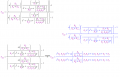
WOWThe Electrician's friend here. Here is what I get from LTspice:View attachment 162733 View attachment 162734
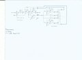
For the schematic I used a hierarchical subcircuit for each slider section. I think you had a typo for one of the resistor values, so I changed it to achieve equal EQ for all sections. (You're welcome.)")
Thanks alot man. I'm really new to this spice thing so there's alot for me to learn about this still (I ha no idea you could even model the sliders in spice like that)
Gonna take tonight to go through everything and understand what you did...im seeing if statements next to the filter stages so i'm guessing you modelled them as purely theoretical :O ....which would leave it up to me to determine what op-amps to use to get a close enough response to the theoretical model. I'd have to play around with components in the lab to determine this most likely I guess.
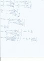
Funny thing is I was in the lab trying to understand this today and my friends saw it and they recognized it was an admittance matrix (They branched off into power systems...I branched into computer systemsI'm doing a nodal analysis of the complete circuit, with the nodal equations in matrix format. Thank goodness for modern mathematical software. The amount of number crunching would not be possible without it. My laptop takes about 5 seconds to solve the matrix numerically, and a few seconds to plot the response. A symbolic solution is possible, but it takes about 15 minutes to do it!!!
I may add a couple more filters, but as it stands now I think the circuit is behaving as expected.
Is the response you show with alternate filters set for boost, cut, boost, cut, boost, cut, etc.? I don't know why you get the irregular response; mine seems perfectly regular if, for example all the bands are set for the same amount of boost or cut.
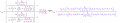
Here's how I set things up; I'm not showing the plotting code (the easy part):
View attachment 162710
...i'd spend some time this week trying to learn this method because it looks pretty cool ) I guess this explains all the errors I was having beforeI'm recalling a problem I had with this analysis which may be a clue to your difficulty. When I started the analysis of this circuit I only had a single filter, and everything was working ok.
When I added the second filter, Mathematica (which I'm using to do the number crunching) reported that my admittance matrix was singular. It took me a while to find the problem. I was using standard double precision floating point arithmetic. This means using about 17 digit floating point arithmetic. It turns out that the circuit is large enough that some of the internal calculations were over/under flowing the arithmetic. Mathematica allows for arithmetic other than floating point. The other method is rational arithmetic--all numeric quantities are represented as fractions with integer numerator and denominator. This is essentially "infinite" precision arithmetic; there's no roundoff error. When I switched to this method, the problem of singularity of the admittance matrix went away.
I was getting this problem with the addition of the second filter. Just imagine what would happen with 15 filters! I don't know if LTSpice can do rational arithmetic, but it's possible that it may be having problems with its floating problem arithmetic when solving such a large problem.
I'd never have figured that out...I was starting to doubt the design.
My next phase of the project based on the requirements would be to replace all potentiometers with digital pots and implement a digital interface to control the boosting and cutting of the various bands using a micro-controller(The part i've been looking forward too). Oh with a VU meter in the digital interface as well.
Will post my designs/approach for this soon, as well as for the system's power supply.