Help Needed - Basic Sensor Board

Thread Starter

CurtCircuit

Joined Dec 19, 2025
18
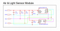
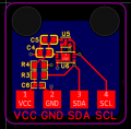
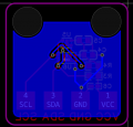
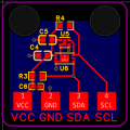
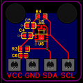
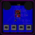
This is the first PCB I've ever designed, if anyone could look over it and let me know what I could add, something I should fix, or a more clean way to organize the design that would be awesome! I used decoupling capacitors near the power entry for the board, and also near the power for each of the two sensors. This board is meant to wire up to an ESP32 Devkit C.

Schematic.png

Schematic.pngPCB_Layout.png2D_Top_PCB.png2D_Bottom_PCB.png
 

WBahn

Joined Mar 31, 2012
32,702
Have YOU looked at it to see if there's anything obvious?

1766194491081.png

Why route a trace around another pad when you can go straight to it?

You do this in another place, as well.

Think twice before putting vias on pads. It can make it hard to solder the components down. Not only is the surface of the pad not smooth, but you have a heatsink firmly connected to your big ground plane.

I'd also recommend against having acute angles in your resist as it can be a manufacturability issue (at least it used to be, don't know about today).

I'd place my C3 cap like the following:

1766194968723.png

Also, make your power traces as large as possible. No reason to skimp if you don't have to.
 

Thread Starter

CurtCircuit

Joined Dec 19, 2025
18
Have YOU looked at it to see if there's anything obvious?

View attachment 360814

Why route a trace around another pad when you can go straight to it?

You do this in another place, as well.

Think twice before putting vias on pads. It can make it hard to solder the components down. Not only is the surface of the pad not smooth, but you have a heatsink firmly connected to your big ground plane.

I'd also recommend against having acute angles in your resist as it can be a manufacturability issue (at least it used to be, don't know about today).

I'd place my C3 cap like the following:

View attachment 360815

Also, make your power traces as large as possible. No reason to skimp if you don't have to.
Thank you for the feedback! I'm gonna go fix those few things.
 

MrChips

Joined Oct 2, 2009
34,627
Also, think about the function of C1, C2, and C3.

The purpose of C3 is to filter the power supply of the entire circuit.
The purpose of C1 is to decouple the power supply at U3 alone. Keep the traces between C1 and U3 as short as possible.
The same goes for C2 and U4.

To put it differently, the purpose of C3 is to smooth out low frequency variation on the power supply. Hence it has a higher capacitance.
In contrast, the purpose of C1 and C2 is to remove high frequency noise generated by the IC that is closest to it. Hence, you want to reduce any inductance that might be presented by the connecting traces.

For this simple board, none of this really matters. However, it is better to understand and maintain this practice because it becomes essential in more complex circuits.
 

dl324

Joined Mar 30, 2015
18,216
Thanks, I will move the decoupling capacitors closer to the sensors!
I'd rotate C1 180 degrees and C2/C3 90 degrees clockwise. Put the supply ends of C1 and C2 as close to the component power leads as possible because you want the lowest inductance on those nets. I'd use wire connections to GND instead of vias. Same for GND to U4.

Straighten the SDA wire and clean up the routing for SCL.
 
Last edited:

WBahn

Joined Mar 31, 2012
32,702
@CurtCircuit: Is the location of the two sensors fixed, or can they be moved a bit?

This looks like the output of some APR (auto place and route) tool that wasn't reviewed at all.

If they can be moved, then by moving them just a tiny bit the routing can be made much cleaner.

Look at the track coming out of the power pin on U4. Why does it need to come out at an angle from the corner when it could come out straight across to C2 if these were just aligned better.

Why the need for the jog in the track coming up from SDA? If U4 was moved slightly to the left, it could come straight up (or it could come straight up now if it joined the bad toward the right side of it, though I don't like that because it isn't "pretty" -- personal preference).

The single track on the bottom of the board is much more complex than it needs to be and needlessly crowds the SDA track to U3.

The two sensors are on an SDA/SCL bus. Make the routing look like that's the case.
 

Thread Starter

CurtCircuit

Joined Dec 19, 2025
18
I redid the schematic and PCB design. I added pull-up resistors for the SDA and SCL nets. I cleaned up the schematic to be easier to read. I also did the traces manually this time (I did use auto-routing before). I moved the decoupling capacitors closer to the sensors and packed everything a bit closer together to shorten traces. I didn't make the power trace wider because the two sensors on this board require a very small current and the 0.254mm width the traces are currently is more than sufficient. Thank you all so much for the advice, if anyone has any other tips please let me know. Here are the updated designs:
 

Attachments

MrChips

Joined Oct 2, 2009
34,627
You have the ground side of C5 connected to the ground side of C4.
Again, you are adding additional inductance whereas your objective is to eliminate inductance wherever possible. Each capacitor should have a direct connection to a low impedance GND track. It doesn’t have to be a ground plane.

If you moved R4 to the other side of U5 you could eliminate two vias.
 

Thread Starter

CurtCircuit

Joined Dec 19, 2025
18
You have the ground side of C5 connected to the ground side of C4.
Again, you are adding additional inductance whereas your objective is to eliminate inductance wherever possible. Each capacitor should have a direct connection to a low impedance GND track. It doesn’t have to be a ground plane.

If you moved R4 to the other side of U5 you could eliminate two vias.
Does this look cleaner, I gave each decoupling capacitor their own connect to the ground plane. I also moved the R4 pull-up to the top.
 

Attachments

ronsimpson

Joined Oct 7, 2019
4,645
They way we made PCBs 40 years ago is not what we do today. My first board was more than 50 years ago. I think I was in 3rd grade. Look at C6. Years ago, sharp corners were hard to get the board to etch right. C6 Right side has a sharp corner. C6 Left side I changed to not do that. (sorry paint does not edit well)
To get CAD to make that trace I would click on C6 Left pad, move to the bottom corner of the pad and click again, drop down to the top right corner of VCC-1, click, now go to the center of pad and end the trace.
1766247305454.png
Next comment is about the spacing on C4, top of the picture. Your line reduces the spacing between lines. If there will be a board short it will be there. I drew a line that does not decrease the spacing. (don't do the rounded corners) I just want to say drop down first a little then head left to get away from C4.

Last comment: I have made things that made millions of boards/month. A VIA cost money. In the old days, enough you could count it. You probably will not make high volumes. Most board houses do not count the VIAs on runs of less that 10,000 boards. My point, they will not charge you more if you had 100 vias in this board. Every via is a chance of a failure. I often add backup VIAs if the current is high or if a good ground connection is important for noise. (I think you don't need to) There is nothing wrong in putting 2,3 or 4 VIAs on the GND pad.

Every one of us has different experiences, red different books, worked with different companies. We do things differently. You are free to make your set of laws. Do what you want! On PCB design, us old men often disagree. Read our comments, learn why, then though out 1/2 of what we say, and do what looks good to you.
 

Thread Starter

CurtCircuit

Joined Dec 19, 2025
18
They way we made PCBs 40 years ago is not what we do today. My first board was more than 50 years ago. I think I was in 3rd grade. Look at C6. Years ago, sharp corners were hard to get the board to etch right. C6 Right side has a sharp corner. C6 Left side I changed to not do that. (sorry paint does not edit well)
To get CAD to make that trace I would click on C6 Left pad, move to the bottom corner of the pad and click again, drop down to the top right corner of VCC-1, click, now go to the center of pad and end the trace.
View attachment 360871
Next comment is about the spacing on C4, top of the picture. Your line reduces the spacing between lines. If there will be a board short it will be there. I drew a line that does not decrease the spacing. (don't do the rounded corners) I just want to say drop down first a little then head left to get away from C4.

Last comment: I have made things that made millions of boards/month. A VIA cost money. In the old days, enough you could count it. You probably will not make high volumes. Most board houses do not count the VIAs on runs of less that 10,000 boards. My point, they will not charge you more if you had 100 vias in this board. Every via is a chance of a failure. I often add backup VIAs if the current is high or if a good ground connection is important for noise. (I think you don't need to) There is nothing wrong in putting 2,3 or 4 VIAs on the GND pad.

Every one of us has different experiences, red different books, worked with different companies. We do things differently. You are free to make your set of laws. Do what you want! On PCB design, us old men often disagree. Read our comments, learn why, then though out 1/2 of what we say, and do what looks good to you.
Thank you for the tips I just fixed the line going from R3 to C4, and the sharp turns from the pads to C6. I also made the pads on the board through holes, I've been told that's easier to solder to than regular surface pads. Now that they're through holes the GND pad connects directly to the copper pour on the bottom side of the board, I think the vias I have now should be fine. Here are the updated layouts:
 

Attachments

MrChips

Joined Oct 2, 2009
34,627
Ah, yes!

How boards are made today is very different from when we laid out artwork with black tape (red and blue for double sided) and etched the boards by hand. However, I still believe in applying the same rules.

1) Don't make a double sided PCB if you can do it with a single sided PCB, even if it requires a couple of jumpers.
2) Don't use a via if you can find a solution without one.
3) Give every track space when space is available.

And finally, PCB layout is called artwork. Treat it as a piece of art that you are proud of making and showing off to others.
 

ronsimpson

Joined Oct 7, 2019
4,645
1) Don't make a double sided PCB if you can do it with a single sided PCB, even if it requires a couple of jumpers.
Most board houses charge the same for single sided as they do for double sided, now. We had a jumper machine that I hated. It was another step in production. More things to go wring. I have had problems with parts pulling out of single sided boards, under vibrations. I had the option of a single sided board with plated through holes, but that is made from a double-sided board.
It might be that my preadjust against single sided boards comes from the cheap board houses that use very think copper and a board made of "cardboard". I know it is not cardboard, but it is nasty. They do not drill the holes but punch them.
2) Don't use a via if you can find a solution without one.
We all have seen VIAs that failed, but I have not seen one in many years. Boards are much better now.
Yes. Sometimes I hide a smiley face under a large capacitor. "unprofessional" Put your name or initials on the board. At least put the date. Some years from now, someone will look at the board with no writing and say, "what the hell is this"
two sensors, use with ESP32 Devkit C, 12/20/25 Curt
RonS.
 

MrChips

Joined Oct 2, 2009
34,627
Of course, PCB houses have tighter tolerances. Today, I am more likely to make my own board by milling on a CNC machine. Hence I make all my pads, tracks, and spacing much wider. Instead of going down below nanometres, I am scaling back up to millimetres. Progress!
 
Top