 Facebook
 Google
 GitHub
 Linkedin
Hey all,
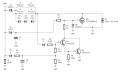
I'm attempting to reverse engineer a PCB I've been given, I'm fairly confident the schematic I've produced is accurate, though I'm having some trouble understanding how it actually operates as I'm not particularly good with analog electronics. For reference this PCB is designed as a dummy electric brake magnet, intended to connect to brake controllers and acting as a fake load, the PWR input is a ~13V variable PWM signal (pulling only around 0.1A at ~13V and close to 100% PWM from my measurements).
Initially I thought that the gate of the mosfet was being held at a constant voltage which limited it's drain to source current, and thereby limiting the current allowed through the big inductors to ground. But no matter what way I seem to approach analysing it, that doesn't seem to work, and neither have the other theories I've toyed with.
Attachments
-
 39.8 KB Views: 45


