Help creating a pcb

MrChips

Joined Oct 2, 2009
34,817
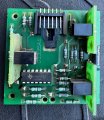
When I first did the schematics I couldn't see the resistor hidden under the cable. I have now renumbered the resistors to take this into account. I have also renumbered the OPTOs to match the 1, 2, 4 numbering on the connector.

Hadaak_schema.jpg
Hadaak_board.jpg

Hadaak_overlay.jpg


Hadaak_PCB_traces.jpg


The attached zip files are:

.gtl = gerber top layer
.gbl = gerber bottom layer
.ovl = top silk screen
.dri = Excellon drill file (_drill.txt)
.sch = Eagle schematics
.brd = Eagle board layout

The PCB manufacturer can use the .brd to extract all the PCB information.
 

Attachments

MrChips

Joined Oct 2, 2009
34,817
I just noticed that the OPTO boards have as strip of copper so that the daughter board is soldered to the mother board.
I can add this if desired.
 

Thread Starter

Hadaak

Joined Jul 17, 2015
52
That’s awsome MisterChips. Very much appreciated.
As for the solder between the motherboard and daughterboard I guess it is there only for bonding. I will check the board again and check for continuity. I would like to add a JST type flat connector like the one on the new board for easy/secure mounting if that’s not too much trouble for you. I cannot use header pin style as that will interfere with the ruler going through the optos.
Thanks again for your help !
 

Attachments

MrChips

Joined Oct 2, 2009
34,817
The original board you showed had no solder mask and no plated through holes. The cable was wired directly to the board.
I made the PCB layout to match that board closely with the cable soldered to the PCB.

To accommodate a connector, the resistors would have to be moved around. The layout of the later board you recently posted is very different from the original board.
 

Thread Starter

Hadaak

Joined Jul 17, 2015
52
No worries then. I will keep the soldered cable and add a connector a few cm further. Thanks again MrChips.
by the way do you see any difference or update between the two boards? I posted the schematics of the latest board earlier in the thread.
 

MrChips

Joined Oct 2, 2009
34,817
No worries then. I will keep the soldered cable and add a connector a few cm further. Thanks again MrChips.
by the way do you see any difference or update between the two boards? I posted the schematics of the latest board earlier in the thread.
I don't see any difference except for the PCB layout.
 
Top