Facebook
 Google
 GitHub
 Linkedin
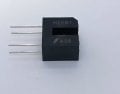
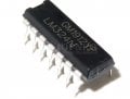
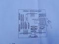
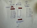
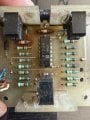
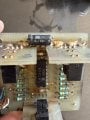
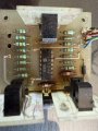
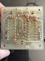
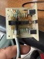
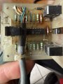
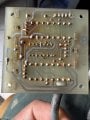
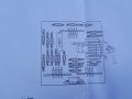
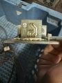
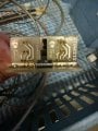
Hi guys. First post here. Anybody willing to help with creating a schematic for this board. One of the photoelctric switches is behaving strangely. It stays closed. This is probably due to some of the resistors which look fried. I thought why not create a new board. Looks simple and would be a breeze to draw for an experienced person but I have never done it. I can try but that will take me some time to learn. Any help would be greatly appreciated. Thanks.
Attachments
-
 1.5 MB Views: 33
 -
 1.4 MB Views: 34
 -
 1.4 MB Views: 32
 -
 530.7 KB Views: 33
 -
 49.8 KB Views: 33
 -
 944.6 KB Views: 29
 -
 1 MB Views: 28