Height Misalignment problem between fine-pitch ICs and the etched copper traces of that PCB.

Thread Starter

Akhil@2k4

Joined May 31, 2024
6
It has been observed that in fine-pitch ICs like QFN, DFN, TQFN (of BTC), there exists a height mis-alignment problem between the lead frame of the fine-pitch ICs and the etched copper connections, as a consequence which leads to problems while PCB assembling (solder voids). Review the Gerber files of some EVMs (Evaluation Manuals) like HMC321alp4e, HMC980lp4etr and find different solutions to solve the above problem.

This was the problem which we are facing with our PCBs, so can anyone please help me with the solution?

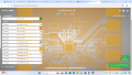
The screenshot of Gerber file of one of the IC was attached, in which we can see that due to the copper beneath the IC, we are facing this issue... So, what do you think the solution could be?
 

Attachments

Thread Starter

Akhil@2k4

Joined May 31, 2024
6
It's not clear what the problem is.. do you mean the PCB isn't flat so the chip doesn't sit properly? Are some pads higher than other pads? Or is it a solder paste problem (not enough paste)?
Thanks for your concern, the PCB is flat, but there is a slight height misalignment between the IC's terminals and the pads. This was reported by one of our vendors that they facing issue while assembling the PCB. We are thinking that this might be due to the copper beneath the IC, which is giving the extra height to the IC.
 

MrSoftware

Joined Oct 29, 2013
2,273
The copper under the IC should be the same height as the pads. Is there maybe solder mask where there shouldn't be? Is the copper under the IC supposed to be a pad that gets paste? Or is it a ground plane that is supposed to have solder mask over it?
 

Thread Starter

Akhil@2k4

Joined May 31, 2024
6
The copper under the IC should be the same height as the pads. Is there maybe solder mask where there shouldn't be? Is the copper under the IC supposed to be a pad that gets paste? Or is it a ground plane that is supposed to have solder mask over it?
If we can see the Gerber file screenshot, there is a solder opening at the IC, so only copper will be under the IC. No, copper under IC is not supposed to be a pad that gets paste.
 

MrSoftware

Joined Oct 29, 2013
2,273
It sounds really odd to have an exposed copper pad under the chip that doesn't get paste. Is the bottom side of the chip an exposed pad? Can you post a clear picture of the chip bottom, the bare board and the chip sitting on the board showing the issue?
 

Thread Starter

Akhil@2k4

Joined May 31, 2024
6
It sounds really odd to have an exposed copper pad under the chip that doesn't get paste. Is the bottom side of the chip an exposed pad? Can you post a clear picture of the chip bottom, the bare board and the chip sitting on the board showing the issue?
The problem is, i can't share the picture, as per company norms... The problem is that the "lead-frame" of the IC is not properly connecting with the copper pads, as it is mounted on the copper pad, which has the same thickness of copper traces. Hence, the problem of height is being a problem(as far as I understood).
 

Thread Starter

Akhil@2k4

Joined May 31, 2024
6
I propose once again, the answer that you ignored before: Could it be too much solder paste on that pad?
My apologies for my ignorance, yeah most probably that could be the reason. Because we were reported from our vendor that they were facing an issue while assembling, maybe because of "Solder Voids" at the joints. So, can you give a solution for this?
And moreover, do you think "usage of Solder Preforms could solve our problem"?
 

panic mode

Joined Oct 10, 2011
4,864
looks like wrong footprint was used. pad under the IC is required in some cases, typically for cooling. but in your case IC does not have the bottom pad, so gerbers are wrong, and paste is applied. that creates bubble of solder under the IC which is lifting the IC and causing misalignment.
the solution is to create new gerbers/stencil to prevent deposit of the paste under the IC... or solder the ICs by hand
 

nsaspook

Joined Aug 27, 2009
16,249
looks like wrong footprint was used. pad under the IC is required in some cases, typically for cooling. but in your case IC does not have the bottom pad, so gerbers are wrong, and paste is applied. that creates bubble of solder under the IC which is lifting the IC and causing misalignment.
the solution is to create new gerbers/stencil to prevent deposit of the paste under the IC... or solder the ICs by hand
That's the root cause solution, use the right footprint for each device. Another that I use when hand soldering a IC with pads it to use a plated hole from the pad layer to a bottom ground layer. Lightly paste the pad, heat and then reflow with an iron using the hole. A plating finish like ENIG instead of a solder wash makes PCB device pad alignment much more accurate.
1717642352037.png
1717605924541.png
1717606073579.png
 
Last edited:

MrSoftware

Joined Oct 29, 2013
2,273
Footprint was going to be my next suggestion. There will be a recommended footprint in the datasheet for the part. Compare that carefully to your footprint and see if you notice any differences.
 
Top