Heat dissipation vias in high power/high frequency PCB?

Thread Starter

SiCEngineer

Joined May 22, 2019
442
Hi All,

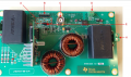
Ihave been studying the attached PCB design image and notice there are a lot of holes in the PCB which look like vias. But they are plated, and seem to be on the power planes. I believe they may be for power dissipation of some sort, but they are also included in the lower voltage/power section of the board so I am not so sure.

Please advise.

https://www.ti.com/lit/ug/snou140a/snou140a.pdf see page 12.
 

Attachments

Irving

Joined Jan 30, 2016
3,880
I'm sure I've seen this posted elsewhere on AAC - duplicate threads are best avoided.

Vias are almost always plated otherwise they serve little purpose. The bulk of the vias are to share high current loading between tracks mirrored on 2 layers, e.g. down near the VDC connector. Vias are inherently a higher resistance than the track hence the need for an array of them. There are also thermal vias, typically between ground planes, to move heat away from ICs to external layers to provide heatsinking. In many cases the vias do both.
 

Thread Starter

SiCEngineer

Joined May 22, 2019
442
I'm sure I've seen this posted elsewhere on AAC - duplicate threads are best avoided.

Vias are almost always plated otherwise they serve little purpose. The bulk of the vias are to share high current loading between tracks mirrored on 2 layers, e.g. down near the VDC connector. Vias are inherently a higher resistance than the track hence the need for an array of them. There are also thermal vias, typically between ground planes, to move heat away from ICs to external layers to provide heatsinking. In many cases the vias do both.
Apologies if it was a duplicate, I did search and didn't find an answer to my questions. I understand the ones near VCC however unsure still of the very small and very uniformly distributed ones in the ground copper pour near the lower power components. This is only a two layer board so I don't see how they are heatsinking between ground planes?
 

Irving

Joined Jan 30, 2016
3,880
Apologies if it was a duplicate, I did search and didn't find an answer to my questions. I understand the ones near VCC however unsure still of the very small and very uniformly distributed ones in the ground copper pour near the lower power components. This is only a two layer board so I don't see how they are heatsinking between ground planes?
Its a 4 layer board - fig 15 & 16 are the inner layers...
 

Thread Starter

SiCEngineer

Joined May 22, 2019
442
Its a 4 layer board - fig 15 & 16 are the inner layers...
Yes, the inner layers for the daughterboard. I am also talking about the 2-layer motherboard as this is what I will be designing. I have two of the motherboards which will act as my power converters. I need to now design the motherboard such that I can connect my voltage/current sensors, input voltage and transformer. I decided it was no point re-designing the daughterboard for my app.
 

Deleted member 115935

Joined Dec 31, 1969
0
Its generally good practice, to "bolt" all grounds together on a board in as many places as possible / practical.
 

Thread Starter

SiCEngineer

Joined May 22, 2019
442
Its generally good practice, to "bolt" all grounds together on a board in as many places as possible / practical.
Even those grounds which are belonging to other isolated parts of the board?

For example, would you connect the power ground to an isolated 12V supply in the case of this board?
 

Thread Starter

SiCEngineer

Joined May 22, 2019
442
If its isolated, and you connect it , its no longer isolated.
so what exactly is ground in this sense? I will connect my current limiting power supply ground to the power ground of the PCB... if this is not connected to the other grounds, then what exactly makes this isolated ground “grounded” if this makes sense? Is it just because it’s connected to a large copper pour we class it as a ground since it forms a return path? Therefore to have two deprecate grounds we need two copper pours which are separate and not connected at any point?
 

Deleted member 115935

Joined Dec 31, 1969
0
I'm sorry @SiCEngineer

I am now totally confused by what you are asking,
I Think I had better bow out of this,

let some one new have a go
 

Irving

Joined Jan 30, 2016
3,880
It is quite common to separate analog and digital grounds, or to have separate grounds for low current and high current areas of the board to avoid cross-talk and interference.

Yes, they will be connected at some point, but in a defined and controlled way.
 
Top