Ground bounce problems in -48V referenced Flyback Converter

Thread Starter

Chipbox

Joined Aug 13, 2018
16
Hi everyone,
I am building an DC/DC converter for a somewhat unique application, of which I'm running into some problems.

Background:
I am building a 100kHz, 50W flyback converter with some of the following properties:
- Primary lower potential = -48VDC
- Primary input voltage relative to -48VDC = 0VDC (earth ground)
- The transformer operates in DCM.
The secondary of the flyback transformer has its lower potential at 0VDC (earth) whose secondary output voltage can go as high as 300V+.
Everything I described has been designed, built, and tested on a PCB.

Problem:
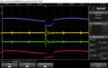
I am having significant "ground" bounce problems at the primary -48VDC power plane downstream of the EMI filter. The "ground bounce" I am referring to is actually a -48VDC bounce, but for sake of convenience, lets refer to the -48V bounce as ground bounce.

The common mode choke at the EMI filter does decrease the amplitude of the bounce at the source, but at the expense of walloping ground bounce with an amplitude of around 100V+ at the -48VDC power plane downstream of the EMI filter. The waveform of the ground bounce directly corresponds to the switching of the MOSFET (as is expected). The common mode choke blocks the dI/dt from the transformer which leaves the current distributed in the power plane, hence the 100V+ bounce.

This bouncing is causing the following problems: 1) heat build-up from switching currents in the -48VDC plane, 2) Sudden turn off the gate driver, 3) high voltage spikes in other control circuitry referenced to the -48VDC plane.

I want to minimize EMI interference at the 48V source, therefore an EMI filter is necessary. On the other hand, a strong EMI filter traps the switching currents in the -48VDC power plane, causing a host of problems.

Question:
What recommendations would you have for my next PCB prototype to minimize my 'ground' bounce problem? I am thinking about adding a large heatsink to the bottom of the board at a few entry points to the -48VDC plane. I can also make my -48V plane in my PCB even larger although it takes a fairly large surface area already. What are other ideas you might have? What are recommended practices to follow in such a case?
 

Attachments

crutschow

Joined Mar 14, 2008
34,285
Does the PCB has a good ground plane for the common?
Are there low impedance ground and power connections between all the devices?
 

ebp

Joined Feb 8, 2018
2,332
What is the signal reference point for the scope traces? The blue and magenta traces look identical and abominably huge (as in, "I don't believe they are real" huge). They also appear to be very nearly identical - which one would expect at high frequency because the supply and common should be at the same potential at high frequency if the capacitors between are good.

What is the weight of copper for the ground plane (which I disparage in subsequent remarks)?

It would help to turn up the scope timebase to reveal detail. There is no value in having nearly six identical copies of the waveforms - it just obscures detail. Making the blue and magenta traces adjacent would make comparison of them easier.

What is putting the trash at nearly four times the switching fundamental on the waveforms?

The values in the leakage inductance discharge circuit are very strange. A 10 W resistor in a 50 W supply is reminiscent of load-line shaping networks from the days of bipolar switches in flybacks. With 10 ohms, you are probably significantly increasing the time it takes to discharge the leakage inductance and very likely eating substantial energy that should be going to the output side.

Foil all over a surface of a PCB is not really a ground plane for a switcher and making connections to it without regard for where current is going is hazardous. High frequency current will flow under the current carrying conductors on the top side - which is usually a good thing, but it also means there can be potential differences that cause grief. Sometimes it is better to keep certain current paths out of the plane. For example, it is probably better to keep the connection between the FET source and the gate driver out of the plane unless you've looked carefully at where the main current is going. If the driver's connection to the source goes into the plane very close to where the source does, things will probably be OK. Expect trouble if it is connected elsewhere.

Look carefully at the docs to which Dana linked. With switchers, unless you are using active probes with very low (not more than 1 or 2 picofarads) tip capacitance, you cannot use a "ground lead" for the probe - it is too inductive and its inductance resonates with the tip capacitance. (You can use it, but what you see won't be "real".) A probe tip grounder with a good, low-capacitance passive attenuator probe will do reasonably well. They are difficult to use and a slip of the grounder can be disastrous if any other probe grounds are connected. Connecting multiple probe grounds to different places in the circuit introduces more uncertainty. It can be extremely difficult to distinguish reality from artifact with probing switchers. I made a point of making points for tip grounders - vias to back-side ground or void dots in solder mask on top-side ground, sprinkled around the board in areas where I might want to probe (which means pretty much everywhere on a prototype). A small mound of solder with a centre dimple made with a fine awl (grind a piece of 1 mm piano wire to a point) makes a pretty good slip-resistant place for the tip of the tip grounder. Be grateful you input side isn't at 400 volts.

I assume your circuit is simplified. I have an abhorrence for switchers that don't have cycle-by-cycle current limiting for the switch.
 

Thread Starter

Chipbox

Joined Aug 13, 2018
16
Hello,

Thank you all for your responses.

I am aware not all capacitors are equal. I made a point of adding film capacitors in parallel with the input and output caps to mitigate some higher frequency components.

Regarding “good ground plane for the common”, please see an image of my PCB. The yellow is the -48V plane. I am aware that the common surface area should be maximized, although I believe I made a mistake in not extending the -48V common plane to where some of the control circuitry is located using more direct vias and an even larger flood. Note I also added a jumper between pins 4 and 8 (both common) on my driver so they could be at a closer potential.

Regarding probes, I am using 10:1 passive rated to 500MHz, 10Mohm/11pF. I chose to disconnect the ground tips when conducting the tests, being cognizant of the uncertainty and potential undesirable currents resulting from such an operation. Regarding whether what I’m seeing is “real”, is it plausible to you that the EMI filter could be the trouble-maker instead – blocking switching currents from returning to the source while distributing it instead to the rest of the PCB plane, increasing the temperature of the copper pours which, unsurprisingly to me, did start to get hot as measured with an IR thermometer. And this even includes the copper traces where the low voltage control circuitry is located – which is obviously not good.

“It can be extremely difficult to distinguish reality from artifact with probing switchers.” – This comment caught my attention. Would you suggest that passive probes are perhaps insufficient for the application, and invest the money in an active or differential probe instead? I believe the math function on the scope would do the same job as well – although tedious. On top of Dana’s recommended app notes, what else do you think I should know about? My switcher is a fairly average (or even low) switching frequency of 100kHz. I know some go up to a few MHz which is not my case. Even then, would a passive probe still not be sufficient for an fs = 100kHz and rise/fall times on the order of dozens of ns? I thought active probes are applied more in ~500MHz+ RF circuits.

I agree entirely with you, @ebp regarding the large blue and magenta traces. This is why I made this post in the first place. Copper is 1oz. Not shown in the circuit diagram, but I am using a CUI PYB30-Q48-T512 elsewhere in my circuit; which from the datasheet has an fs = 400kHz that corresponds perfectly with the oscilloscope readings. What is peculiar however is that the according to the CUI datasheet, the maximum ripple and noise shouldn’t be more than 100mVpk-pk.

Regarding the primary clamp, you are absolutely correct. It was eating up tons of energy. From reading multiple app notes, I was always under the impression that having a primary clamp to reduce ringing was good practice. Early experiments had substantial primary ringing but with my latest prototype I got rid of most of it for now. The ringing isn’t nearly as pronounced as previous prototypes (ie: breadboards, which I determined somewhat late are quite insufficient for switchers). The snubber on the secondary is important however, it cleaned up large ringing on the secondary diode with very little heat dissipation.

I have a current limiting sensors on my load side. I didn’t add one to the primary switch side. From experimentation, it appeared as if the IRS2304 is a good driver so that’s what I used. Honestly, I never considered current limiting on the primary. What sort of circuitry would you recommend for this functionality? Perhaps even what driver to use, if that driver would have this functionality already built-in? Note that I need an output voltage rating of at least 500V as well – which the 2304 and many others can provide.

I've attached a closeup of the same waveform as well.

“Be grateful you input side isn't at 400 volts.” – agreed. As someone still independently learning about SMPS', I’m a happy camper in that regard!
 

Attachments

ebp

Joined Feb 8, 2018
2,332
I'm going to respond piece by piece in a few posts.

"Snubber" on the primary:
Usually you must use some explicit means of discharging the leakage inductance in a flyback converter. At lower power, with the right FET, you can rely on the repetitive avalanche handling capability of the FET, but this is actually getting somewhat less practical because newer FETs have smaller dies for the same current and voltage ratings and small dies translate to lower avalanche energy capability.

The waveform you will see at the drain when the FET turns off has several distinct features.

The first is a high voltage "spike." This is due to the leakage inductance (that is, inductance in the "primary" due to magnetic flux that doesn't couple effectively to the "secondary"). This is what the snubber is for. The objective is to put enough of the energy from the spike "somewhere" so the FET voltage rating isn't exceeded (if you aren't using the avalanche capability). In an RCD snubber, typically you would use a moderately large capacitor (still in pF to nF range) to dump the energy into. You generally leave a little of the spike simply to be sure you aren't eating energy that should be going to the output. You select a resistor of a value low enough to discharge the energy stored in the cap during the remainder of the switching period. Sometimes a transient-suppressor "power zener" can be used to good effect for dealing with at least part of the leakage inductance energy. This sort of snubber puts a hard limit on the peak voltage. The total energy that has to be handled doesn't change. A combination of an RC snubber and a TVS can be quite effective.

Following the spike there will be a fairly flat voltage plateau. During this time, the energy stored in the inductor is being transferred to the output. The two-winding inductor is actually behaving as a transformer during that time - the secondary voltage is referred back to and "stacked upon" the primary voltage by the turns ratio of the inductor. You don't want to do anything that will interfere during this time. The voltage of this plateau is what determines the voltage rating required for the FET - or vice versa - sometimes the turns ratio of the inductor is deliberately fiddled to make the the plateau voltage compatible with the FETs rating, but there are limits to what is practical. Of course you still have to consider any remnant of the the leakage inductance spike voltage.

With a flyback in DCM, the plateau will be followed by ringing. The ringing starts when virtually all of the energy stored in the inductor has been delivered to the the output and the output diode quits conducting. Capacitances including the FET and the winding then resonate with winding inductance and ring down the last bit of energy. There is very little energy being shifted about in this ringing, so it is typically just ignored. In CCM, the FET switches on before the end of the plateau.
 

ebp

Joined Feb 8, 2018
2,332
I'm posting this as-is. I started writing & had to do something. I don't want' it to evaporate, but I haven't proof read it and it isn't quite complete as far as I had intended. I will return to clean it up, but probably half a day from posting time.

QUESTION: I'm still not clear on what point was used for the ground for the scope for the waveforms.


Probes:

Active probes actually have very limited use in switchers unless you get a type that has attenuators that can be added. I think they have become quite a rarity. Without an attenuator, most active probes have very limited input voltage range. They are useful in control circuitry running at a few volts and for looking at signals from current sense resistors and the like.

The probes you have are about as good as high-impedance passive probes get in terms of capacitance at the tip. For many signals in switchers, the capacitive loading, as such, isn't going to change circuit behavior. The issue really is that the energy that goes into charging and discharging that capacitance has to flow through the ground lead inductance and it is the resonance that makes signals often look worse than they are. This is why using a tip grounder makes a very big difference.

Another complication is the fact the whole scope common make a capacitor to "everywhere", so you can get some current in the probe ground and shield even with the tip disconnected. It is not unusual in a switcher to connect the ground lead to the circuit under test, put the probe tip right on the same ground point in the circuit, and still see crud on the scope screen. That's a little test that is worth doing every time you see what looks like a noisy signal.

Traditional differential probes are expensive and again have very limited common mode and differential mode voltage range. There are some diff probes that have input leads like multimeter leads and large voltage handling capability. I've seen bandwidths of 100 MHz claimed. The big question I have is how good the common mode rejection is in the megahertz range. These probes are comparatively inexpensive.

I still don't known what point you are using for the scope ground for the waveforms. If it is on the input side of the input filter, then none of the waveforms mean much of anything in terms of what is going on in the main circuit.

Input filter:
Normally a capacitor would be placed right across the input to turn residual differential noise coming out of the switcher into common mode. This also reduces the vagueries of source impedance that arise from input wiring inductance. It is more common to see the common mode choke at the input and diff mode chokes in-board of the CM choke. The objective would be to attenuate the differential mode noise originating in the switcher into common mode, then reduce the remaining common mode as much as possible before "letting it out" onto the supply conductors.
 

Thread Starter

Chipbox

Joined Aug 13, 2018
16
Q: "I'm still not clear on what point was used for the ground for the scope for the waveforms."
A: The scope ground was connected to the 0VDC earth ground. The ground clips to each probe were disconnected completely.

Q: "If it is on the input side of the input filter, then none of the waveforms mean much of anything in terms of what is going on in the main circuit."
A: I agree and am aware of what you mean. To check individuals signals (eg: 100kHz low voltage carrier) referenced to the PCB -48VDC "common" plane, I often used the math:subtract function on my oscilloscope to understand what is happening “locally”.

There is a caveat to this discussion we haven't talked about much: even after looking at results from such a subtraction, voltage spikes started popping up in the common references of the -48VDC referenced analog circuitry. I noticed this in the 100kHz carrier for example. I suspect it could be caused by way in which the primary leakage currents from the transformer circulate in the PCB -48V plane. This is where, I believe, the PCB layout design of the -48VDC plane becomes critical. I’m wondering how the PCB plane I currently have should be optimized further. I will probably make the -48VDC flood even larger, and use more vias for the -48V referenced digital/analog chips. Based on my PCB screenshot, would you have more ideas, suggestions? I entertained the idea of heatsink, or some other type of metal plate, connected to the -48VDC plane on the bottom of the PCB. Not sure whether that's a good idea, but using an IR gun I noticed the -48VDC plane was starting to get hot. There is also a possible issue of EMI emanating from the absolutely fluctuating (wrt earth), but locally fairly constant 0/48V planes at the output of the EMI – acting as antennas of course and being their own source of EMI. Absolutely speaking, the voltage amplitude is considerable, but at somewhat low frequency (~100kHz).

Would you recommend a better place to put my ground clip if not at earth or EMI input? Example: I’m not certain it would be wise to place it at the high potential output of the EMI filter.

On your input filter comment, did I understand you correctly in the redrawn EMI filter I attached to this post?

Comment: "It is not unusual in a switcher to connect the ground lead to the circuit under test, put the probe tip right on the same ground point in the circuit, and still see crud on the scope screen. That's a little test that is worth doing every time you see what looks like a noisy signal."
Response: I'm not quite following what you're trying to get at here. Am I reading correctly to check to see if the noise is consistent when referenced to multiple "ground" test points? (ie: check signal integrity of signal wrt wallwart earth, ground at load point, different PCB ground test points etc..)
 

Attachments

ebp

Joined Feb 8, 2018
2,332
I'm guessing this is a telecom application and your input supply has the positive side connected to earth ground without the option of floating it.

This makes it horrendously difficult to scope the circuit with any hope of seeing reality. Math functions will work after a fashion, but with a digital scope it really depends a great deal on how the sampling and math are done. At moderate frequency, usually results are pretty good, but as frequency rises they may be less so. If you want to get some idea of how well you can do, connect both probes to something like the FET's drain and look at the difference (i.e. Channel 1 minus Channel 2). Ideally it should be zero, but I can say with some certainty that it won't be.Before you try this, verify that you are within the voltage rating of your probes at the frequencies (including all components above the fundamental switching frequency) involved. The voltage rating of probes falls at frequency rises, but I suspect that with a 48 V supply you should be well within the probe rating up to many megahertz.

Your blue and magenta waveforms are due to the reactance of the input filter inductors. The spikes on the others are probably 90% due to the fact that the scope ground is only very vaguely at the same potential as the input ground - there is just far too much inductance in a presumably long and ill-defined path.

If I were working on this, I would use a floating DC supply so I could put my scope ground where necessary to look at signals (e.g. ground with tip grounder on FET source and probe tip on gate to look at latter). You are wise to be very cautious about where you connect ground without a floating supply - there's plenty of opportunity for problems.

I do not understand why the plane should be heating up. I would estimate your primary side current to be about 2 to 2.2 amperes RMS at 50 W output, 48 V input, with reasonably good efficiency and switch duty cycle in the 35-40% range. That isn't very much, even with just 1 ounce copper, and certainly isn't very demanding of the FET. The current should be a nice (reasonably) clean triangle wave.

I can't say with any certainty that it really makes any difference in your circuit whether the CM filter is ahead of or after the DM filter. In AC-line powered switchers, the CM filter is invariably closest to the power input, but "Y" capacitors from each side of the line to earth ground are normally used so the overall circuit is somewhat different. If you try the revised version, put a capacitor across the line between the CM and DM inductors. Again, the intent is to take what remains of the DM noise at that point and try to make it CM, so as to get the maximum benefit from the CM choke.

Film caps, if they are "stacked foil" types or wound types with the ends fully metalized are generally pretty good performers to quite high frequency. Ceramic are usually better, but start getting fairly big and expensive if you need 100 V rating and want several microfarads. Beware of types with high dielectric constant (e.g. Z5U, Y5V). They can have abominable negative voltage coefficient of capacitance and can be down to a small fraction of nominal capacitance if you run them anywhere near their rated DC voltage.

The business of "crud" showing up on the scope with the tip of the probe shorted to ground near the tip:
One would expect that the scope trace should be a nice flat line, but it rarely is when there are fast voltage transitions in the circuit. This comes back to the fact that the oscilloscope itself and the probe tip ground are not at the same potential at all frequencies. Usually experienced engineers realize that there is only a single point in any circuit that you can truly (and arbitrarily) call zero volts. I sometimes think there isn't even one point that is zero in a switcher :(.

I'll look over your layout on another computer in the next couple of hours, if I can. The one I'm using at the moment doesn't get along very will with my limited vision. I've made a fool of myself :oops: at least twice on AAC because what I thought I was seeing wasn't what was actually there. It's not so much making myself look a fool again that I wish to avoid as wasting your time and mine with the foolishness.
 

Thread Starter

Chipbox

Joined Aug 13, 2018
16
You guessed it. It is for a telecom application.

I appreciate all the recommendations you give. I can assure you that you don't look like a fool to anyone, and you're certainly not wasting my time. This is good dialogue were having, and I'm learning a lot.
 
Top