Facebook
 Google
 GitHub
 Linkedin
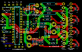
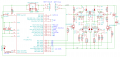
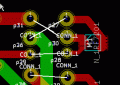
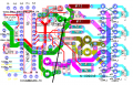
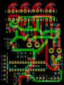
Hi,I have posted a working design without pull ups, why do you want to add them.
BTW: have you received back your components, I posted Monday this week.?

They were suggested earlier in the thread, just checking. It's easier to check now, than wait till I've etched the board.
No components received yet.
C.