Facebook
 Google
 GitHub
 Linkedin
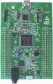
This is a thread about STM32CubeIDE and the STM32F4-Discovery development kit.

Attachments
-
 14.5 KB Views: 11
/* USER CODE BEGIN Header */
/**
******************************************************************************
* @file : main.c
* @brief : Main program body
******************************************************************************
* @attention
*
* <h2><center>© Copyright (c) 2019 STMicroelectronics.
* All rights reserved.</center></h2>
*
* This software component is licensed by ST under Ultimate Liberty license
* SLA0044, the "License"; You may not use this file except in compliance with
* the License. You may obtain a copy of the License at:
* www.st.com/SLA0044
*
******************************************************************************
*/
/* USER CODE END Header */
/* Includes ----------------------*/
#include "main.h"
#include "usb_host.h"
/* Private includes ---------------*/
/* USER CODE BEGIN Includes */
/* USER CODE END Includes */
/* Private typedef --------------------*/
/* USER CODE BEGIN PTD */
/* USER CODE END PTD */
/* Private define -----------------------*/
/* USER CODE BEGIN PD */
/* USER CODE END PD */
/* Private macro -----------------------*/
/* USER CODE BEGIN PM */
/* USER CODE END PM */
/* Private variables ---------------------*/
I2C_HandleTypeDef hi2c1;
I2S_HandleTypeDef hi2s3;
SPI_HandleTypeDef hspi1;
/* USER CODE BEGIN PV */
/* USER CODE END PV */
/* Private function prototypes --------------*/
void SystemClock_Config(void);
static void MX_GPIO_Init(void);
static void MX_I2C1_Init(void);
static void MX_I2S3_Init(void);
static void MX_SPI1_Init(void);
void MX_USB_HOST_Process(void);
/* USER CODE BEGIN PFP */
/* USER CODE END PFP */
/* Private user code --------------------------*/
/* USER CODE BEGIN 0 */
/* USER CODE END 0 */
/**
* @brief The application entry point.
* @retval int
*/
int main(void)
{
/* USER CODE BEGIN 1 */
/* USER CODE END 1 */
/* MCU Configuration---------------------------*/
/* Reset of all peripherals, Initializes the Flash interface and the Systick. */
HAL_Init();
/* USER CODE BEGIN Init */
/* USER CODE END Init */
/* Configure the system clock */
SystemClock_Config();
/* USER CODE BEGIN SysInit */
/* USER CODE END SysInit */
/* Initialize all configured peripherals */
MX_GPIO_Init();
MX_I2C1_Init();
MX_I2S3_Init();
MX_SPI1_Init();
MX_USB_HOST_Init();
/* USER CODE BEGIN 2 */
/* USER CODE END 2 */
/* Infinite loop */
/* USER CODE BEGIN WHILE */
while (1)
{
/* USER CODE END WHILE */
MX_USB_HOST_Process();
/* USER CODE BEGIN 3 */
}
/* USER CODE END 3 */
}
/**
* @brief System Clock Configuration
* @retval None
*/
void SystemClock_Config(void)
{
RCC_OscInitTypeDef RCC_OscInitStruct = {0};
RCC_ClkInitTypeDef RCC_ClkInitStruct = {0};
RCC_PeriphCLKInitTypeDef PeriphClkInitStruct = {0};
/** Configure the main internal regulator output voltage
*/
__HAL_RCC_PWR_CLK_ENABLE();
__HAL_PWR_VOLTAGESCALING_CONFIG(PWR_REGULATOR_VOLTAGE_SCALE1);
/** Initializes the CPU, AHB and APB busses clocks
*/
RCC_OscInitStruct.OscillatorType = RCC_OSCILLATORTYPE_HSE;
RCC_OscInitStruct.HSEState = RCC_HSE_ON;
RCC_OscInitStruct.PLL.PLLState = RCC_PLL_ON;
RCC_OscInitStruct.PLL.PLLSource = RCC_PLLSOURCE_HSE;
RCC_OscInitStruct.PLL.PLLM = 8;
RCC_OscInitStruct.PLL.PLLN = 336;
RCC_OscInitStruct.PLL.PLLP = RCC_PLLP_DIV2;
RCC_OscInitStruct.PLL.PLLQ = 7;
if (HAL_RCC_OscConfig(&RCC_OscInitStruct) != HAL_OK)
{
Error_Handler();
}
/** Initializes the CPU, AHB and APB busses clocks
*/
RCC_ClkInitStruct.ClockType = RCC_CLOCKTYPE_HCLK|RCC_CLOCKTYPE_SYSCLK
|RCC_CLOCKTYPE_PCLK1|RCC_CLOCKTYPE_PCLK2;
RCC_ClkInitStruct.SYSCLKSource = RCC_SYSCLKSOURCE_PLLCLK;
RCC_ClkInitStruct.AHBCLKDivider = RCC_SYSCLK_DIV1;
RCC_ClkInitStruct.APB1CLKDivider = RCC_HCLK_DIV4;
RCC_ClkInitStruct.APB2CLKDivider = RCC_HCLK_DIV2;
if (HAL_RCC_ClockConfig(&RCC_ClkInitStruct, FLASH_LATENCY_5) != HAL_OK)
{
Error_Handler();
}
PeriphClkInitStruct.PeriphClockSelection = RCC_PERIPHCLK_I2S;
PeriphClkInitStruct.PLLI2S.PLLI2SN = 192;
PeriphClkInitStruct.PLLI2S.PLLI2SR = 2;
if (HAL_RCCEx_PeriphCLKConfig(&PeriphClkInitStruct) != HAL_OK)
{
Error_Handler();
}
}
/**
* @brief I2C1 Initialization Function
* @param None
* @retval None
*/
static void MX_I2C1_Init(void)
{
/* USER CODE BEGIN I2C1_Init 0 */
/* USER CODE END I2C1_Init 0 */
/* USER CODE BEGIN I2C1_Init 1 */
/* USER CODE END I2C1_Init 1 */
hi2c1.Instance = I2C1;
hi2c1.Init.ClockSpeed = 100000;
hi2c1.Init.DutyCycle = I2C_DUTYCYCLE_2;
hi2c1.Init.OwnAddress1 = 0;
hi2c1.Init.AddressingMode = I2C_ADDRESSINGMODE_7BIT;
hi2c1.Init.DualAddressMode = I2C_DUALADDRESS_DISABLE;
hi2c1.Init.OwnAddress2 = 0;
hi2c1.Init.GeneralCallMode = I2C_GENERALCALL_DISABLE;
hi2c1.Init.NoStretchMode = I2C_NOSTRETCH_DISABLE;
if (HAL_I2C_Init(&hi2c1) != HAL_OK)
{
Error_Handler();
}
/* USER CODE BEGIN I2C1_Init 2 */
/* USER CODE END I2C1_Init 2 */
}
/**
* @brief I2S3 Initialization Function
* @param None
* @retval None
*/
static void MX_I2S3_Init(void)
{
/* USER CODE BEGIN I2S3_Init 0 */
/* USER CODE END I2S3_Init 0 */
/* USER CODE BEGIN I2S3_Init 1 */
/* USER CODE END I2S3_Init 1 */
hi2s3.Instance = SPI3;
hi2s3.Init.Mode = I2S_MODE_MASTER_TX;
hi2s3.Init.Standard = I2S_STANDARD_PHILIPS;
hi2s3.Init.DataFormat = I2S_DATAFORMAT_16B;
hi2s3.Init.MCLKOutput = I2S_MCLKOUTPUT_ENABLE;
hi2s3.Init.AudioFreq = I2S_AUDIOFREQ_96K;
hi2s3.Init.CPOL = I2S_CPOL_LOW;
hi2s3.Init.ClockSource = I2S_CLOCK_PLL;
hi2s3.Init.FullDuplexMode = I2S_FULLDUPLEXMODE_DISABLE;
if (HAL_I2S_Init(&hi2s3) != HAL_OK)
{
Error_Handler();
}
/* USER CODE BEGIN I2S3_Init 2 */
/* USER CODE END I2S3_Init 2 */
}
/**
* @brief SPI1 Initialization Function
* @param None
* @retval None
*/
static void MX_SPI1_Init(void)
{
/* USER CODE BEGIN SPI1_Init 0 */
/* USER CODE END SPI1_Init 0 */
/* USER CODE BEGIN SPI1_Init 1 */
/* USER CODE END SPI1_Init 1 */
/* SPI1 parameter configuration*/
hspi1.Instance = SPI1;
hspi1.Init.Mode = SPI_MODE_MASTER;
hspi1.Init.Direction = SPI_DIRECTION_2LINES;
hspi1.Init.DataSize = SPI_DATASIZE_8BIT;
hspi1.Init.CLKPolarity = SPI_POLARITY_LOW;
hspi1.Init.CLKPhase = SPI_PHASE_1EDGE;
hspi1.Init.NSS = SPI_NSS_SOFT;
hspi1.Init.BaudRatePrescaler = SPI_BAUDRATEPRESCALER_2;
hspi1.Init.FirstBit = SPI_FIRSTBIT_MSB;
hspi1.Init.TIMode = SPI_TIMODE_DISABLE;
hspi1.Init.CRCCalculation = SPI_CRCCALCULATION_DISABLE;
hspi1.Init.CRCPolynomial = 10;
if (HAL_SPI_Init(&hspi1) != HAL_OK)
{
Error_Handler();
}
/* USER CODE BEGIN SPI1_Init 2 */
/* USER CODE END SPI1_Init 2 */
}
/**
* @brief GPIO Initialization Function
* @param None
* @retval None
*/
static void MX_GPIO_Init(void)
{
GPIO_InitTypeDef GPIO_InitStruct = {0};
/* GPIO Ports Clock Enable */
__HAL_RCC_GPIOE_CLK_ENABLE();
__HAL_RCC_GPIOC_CLK_ENABLE();
__HAL_RCC_GPIOH_CLK_ENABLE();
__HAL_RCC_GPIOA_CLK_ENABLE();
__HAL_RCC_GPIOB_CLK_ENABLE();
__HAL_RCC_GPIOD_CLK_ENABLE();
/*Configure GPIO pin Output Level */
HAL_GPIO_WritePin(CS_I2C_SPI_GPIO_Port, CS_I2C_SPI_Pin, GPIO_PIN_RESET);
/*Configure GPIO pin Output Level */
HAL_GPIO_WritePin(OTG_FS_PowerSwitchOn_GPIO_Port, OTG_FS_PowerSwitchOn_Pin, GPIO_PIN_SET);
/*Configure GPIO pin Output Level */
HAL_GPIO_WritePin(GPIOD, LD4_Pin|LD3_Pin|LD5_Pin|LD6_Pin
|Audio_RST_Pin, GPIO_PIN_RESET);
/*Configure GPIO pin : CS_I2C_SPI_Pin */
GPIO_InitStruct.Pin = CS_I2C_SPI_Pin;
GPIO_InitStruct.Mode = GPIO_MODE_OUTPUT_PP;
GPIO_InitStruct.Pull = GPIO_NOPULL;
GPIO_InitStruct.Speed = GPIO_SPEED_FREQ_LOW;
HAL_GPIO_Init(CS_I2C_SPI_GPIO_Port, &GPIO_InitStruct);
/*Configure GPIO pin : OTG_FS_PowerSwitchOn_Pin */
GPIO_InitStruct.Pin = OTG_FS_PowerSwitchOn_Pin;
GPIO_InitStruct.Mode = GPIO_MODE_OUTPUT_PP;
GPIO_InitStruct.Pull = GPIO_NOPULL;
GPIO_InitStruct.Speed = GPIO_SPEED_FREQ_LOW;
HAL_GPIO_Init(OTG_FS_PowerSwitchOn_GPIO_Port, &GPIO_InitStruct);
/*Configure GPIO pin : PDM_OUT_Pin */
GPIO_InitStruct.Pin = PDM_OUT_Pin;
GPIO_InitStruct.Mode = GPIO_MODE_AF_PP;
GPIO_InitStruct.Pull = GPIO_NOPULL;
GPIO_InitStruct.Speed = GPIO_SPEED_FREQ_LOW;
GPIO_InitStruct.Alternate = GPIO_AF5_SPI2;
HAL_GPIO_Init(PDM_OUT_GPIO_Port, &GPIO_InitStruct);
/*Configure GPIO pin : B1_Pin */
GPIO_InitStruct.Pin = B1_Pin;
GPIO_InitStruct.Mode = GPIO_MODE_EVT_RISING;
GPIO_InitStruct.Pull = GPIO_NOPULL;
HAL_GPIO_Init(B1_GPIO_Port, &GPIO_InitStruct);
/*Configure GPIO pin : BOOT1_Pin */
GPIO_InitStruct.Pin = BOOT1_Pin;
GPIO_InitStruct.Mode = GPIO_MODE_INPUT;
GPIO_InitStruct.Pull = GPIO_NOPULL;
HAL_GPIO_Init(BOOT1_GPIO_Port, &GPIO_InitStruct);
/*Configure GPIO pin : CLK_IN_Pin */
GPIO_InitStruct.Pin = CLK_IN_Pin;
GPIO_InitStruct.Mode = GPIO_MODE_AF_PP;
GPIO_InitStruct.Pull = GPIO_NOPULL;
GPIO_InitStruct.Speed = GPIO_SPEED_FREQ_LOW;
GPIO_InitStruct.Alternate = GPIO_AF5_SPI2;
HAL_GPIO_Init(CLK_IN_GPIO_Port, &GPIO_InitStruct);
/*Configure GPIO pins : LD4_Pin LD3_Pin LD5_Pin LD6_Pin
Audio_RST_Pin */
GPIO_InitStruct.Pin = LD4_Pin|LD3_Pin|LD5_Pin|LD6_Pin
|Audio_RST_Pin;
GPIO_InitStruct.Mode = GPIO_MODE_OUTPUT_PP;
GPIO_InitStruct.Pull = GPIO_NOPULL;
GPIO_InitStruct.Speed = GPIO_SPEED_FREQ_LOW;
HAL_GPIO_Init(GPIOD, &GPIO_InitStruct);
/*Configure GPIO pin : OTG_FS_OverCurrent_Pin */
GPIO_InitStruct.Pin = OTG_FS_OverCurrent_Pin;
GPIO_InitStruct.Mode = GPIO_MODE_INPUT;
GPIO_InitStruct.Pull = GPIO_NOPULL;
HAL_GPIO_Init(OTG_FS_OverCurrent_GPIO_Port, &GPIO_InitStruct);
/*Configure GPIO pin : MEMS_INT2_Pin */
GPIO_InitStruct.Pin = MEMS_INT2_Pin;
GPIO_InitStruct.Mode = GPIO_MODE_EVT_RISING;
GPIO_InitStruct.Pull = GPIO_NOPULL;
HAL_GPIO_Init(MEMS_INT2_GPIO_Port, &GPIO_InitStruct);
}
/* USER CODE BEGIN 4 */
/* USER CODE END 4 */
/**
* @brief This function is executed in case of error occurrence.
* @retval None
*/
void Error_Handler(void)
{
/* USER CODE BEGIN Error_Handler_Debug */
/* User can add his own implementation to report the HAL error return state */
/* USER CODE END Error_Handler_Debug */
}
#ifdef USE_FULL_ASSERT
/**
* @brief Reports the name of the source file and the source line number
* where the assert_param error has occurred.
* @param file: pointer to the source file name
* @param line: assert_param error line source number
* @retval None
*/
void assert_failed(uint8_t *file, uint32_t line)
{
/* USER CODE BEGIN 6 */
/* User can add his own implementation to report the file name and line number,
tex: printf("Wrong parameters value: file %s on line %d\r\n", file, line) */
/* USER CODE END 6 */
}
#endif /* USE_FULL_ASSERT */
/************************ (C) COPYRIGHT STMicroelectronics *****END OF FILE****//* Infinite loop */
/* USER CODE BEGIN WHILE */
while (1)
{
/* USER CODE END WHILE */
//MX_USB_HOST_Process();
HAL_GPIO_TogglePin(GPIOD, GPIO_PIN_12);
HAL_Delay(250);
/* USER CODE BEGIN 3 */
}
/* USER CODE END 3 */


/* USER CODE BEGIN Header */
/**
******************************************************************************
* @file : main.c
* @brief : Main program body
******************************************************************************
* @attention
*
* <h2><center>© Copyright (c) 2020 STMicroelectronics.
* All rights reserved.</center></h2>
*
* This software component is licensed by ST under BSD 3-Clause license,
* the "License"; You may not use this file except in compliance with the
* License. You may obtain a copy of the License at:
* opensource.org/licenses/BSD-3-Clause
*
******************************************************************************
*/
/* USER CODE END Header */
/* Includes -----------------------------------*/
#include "main.h"
/* Private includes ----------------------------*/
/* USER CODE BEGIN Includes */
/* USER CODE END Includes */
/* Private typedef ------------------------------*/
/* USER CODE BEGIN PTD */
/* USER CODE END PTD */
/* Private define --------------------------------*/
/* USER CODE BEGIN PD */
/* USER CODE END PD */
/* Private macro ---------------------------------*/
/* USER CODE BEGIN PM */
/* USER CODE END PM */
/* Private variables -------------------------------*/
TIM_HandleTypeDef htim4;
/* USER CODE BEGIN PV */
/* USER CODE END PV */
/* Private function prototypes ---------------------*/
void SystemClock_Config(void);
static void MX_GPIO_Init(void);
static void MX_TIM4_Init(void);
/* USER CODE BEGIN PFP */
/* USER CODE END PFP */
/* Private user code --------------------------------*/
/* USER CODE BEGIN 0 */
/* USER CODE END 0 */
/**
* @brief The application entry point.
* @retval int
*/
int main(void)
{
/* USER CODE BEGIN 1 */
/* USER CODE END 1 */
/* MCU Configuration-------------------------*/
/* Reset of all peripherals, Initializes the Flash interface and the Systick. */
HAL_Init();
/* USER CODE BEGIN Init */
/* USER CODE END Init */
/* Configure the system clock */
SystemClock_Config();
/* USER CODE BEGIN SysInit */
/* USER CODE END SysInit */
/* Initialize all configured peripherals */
MX_GPIO_Init();
MX_TIM4_Init();
/* USER CODE BEGIN 2 */
/* USER CODE END 2 */
/* Infinite loop */
/* USER CODE BEGIN WHILE */
while (1)
{
/* USER CODE END WHILE */
/* USER CODE BEGIN 3 */
}
/* USER CODE END 3 */
}
/**
* @brief System Clock Configuration
* @retval None
*/
void SystemClock_Config(void)
{
RCC_OscInitTypeDef RCC_OscInitStruct = {0};
RCC_ClkInitTypeDef RCC_ClkInitStruct = {0};
/** Configure the main internal regulator output voltage
*/
__HAL_RCC_PWR_CLK_ENABLE();
__HAL_PWR_VOLTAGESCALING_CONFIG(PWR_REGULATOR_VOLTAGE_SCALE1);
/** Initializes the RCC Oscillators according to the specified parameters
* in the RCC_OscInitTypeDef structure.
*/
RCC_OscInitStruct.OscillatorType = RCC_OSCILLATORTYPE_HSI;
RCC_OscInitStruct.HSIState = RCC_HSI_ON;
RCC_OscInitStruct.HSICalibrationValue = RCC_HSICALIBRATION_DEFAULT;
RCC_OscInitStruct.PLL.PLLState = RCC_PLL_ON;
RCC_OscInitStruct.PLL.PLLSource = RCC_PLLSOURCE_HSI;
RCC_OscInitStruct.PLL.PLLM = 8;
RCC_OscInitStruct.PLL.PLLN = 50;
RCC_OscInitStruct.PLL.PLLP = RCC_PLLP_DIV4;
RCC_OscInitStruct.PLL.PLLQ = 7;
if (HAL_RCC_OscConfig(&RCC_OscInitStruct) != HAL_OK)
{
Error_Handler();
}
/** Initializes the CPU, AHB and APB buses clocks
*/
RCC_ClkInitStruct.ClockType = RCC_CLOCKTYPE_HCLK|RCC_CLOCKTYPE_SYSCLK
|RCC_CLOCKTYPE_PCLK1|RCC_CLOCKTYPE_PCLK2;
RCC_ClkInitStruct.SYSCLKSource = RCC_SYSCLKSOURCE_PLLCLK;
RCC_ClkInitStruct.AHBCLKDivider = RCC_SYSCLK_DIV1;
RCC_ClkInitStruct.APB1CLKDivider = RCC_HCLK_DIV4;
RCC_ClkInitStruct.APB2CLKDivider = RCC_HCLK_DIV2;
if (HAL_RCC_ClockConfig(&RCC_ClkInitStruct, FLASH_LATENCY_0) != HAL_OK)
{
Error_Handler();
}
}
/**
* @brief TIM4 Initialization Function
* @param None
* @retval None
*/
static void MX_TIM4_Init(void)
{
/* USER CODE BEGIN TIM4_Init 0 */
/* USER CODE END TIM4_Init 0 */
TIM_ClockConfigTypeDef sClockSourceConfig = {0};
TIM_MasterConfigTypeDef sMasterConfig = {0};
TIM_OC_InitTypeDef sConfigOC = {0};
/* USER CODE BEGIN TIM4_Init 1 */
/* USER CODE END TIM4_Init 1 */
htim4.Instance = TIM4;
htim4.Init.Prescaler = 0;
htim4.Init.CounterMode = TIM_COUNTERMODE_UP;
htim4.Init.Period = 1;
htim4.Init.ClockDivision = TIM_CLOCKDIVISION_DIV1;
htim4.Init.AutoReloadPreload = TIM_AUTORELOAD_PRELOAD_DISABLE;
if (HAL_TIM_Base_Init(&htim4) != HAL_OK)
{
Error_Handler();
}
sClockSourceConfig.ClockSource = TIM_CLOCKSOURCE_INTERNAL;
if (HAL_TIM_ConfigClockSource(&htim4, &sClockSourceConfig) != HAL_OK)
{
Error_Handler();
}
if (HAL_TIM_OC_Init(&htim4) != HAL_OK)
{
Error_Handler();
}
sMasterConfig.MasterOutputTrigger = TIM_TRGO_RESET;
sMasterConfig.MasterSlaveMode = TIM_MASTERSLAVEMODE_DISABLE;
if (HAL_TIMEx_MasterConfigSynchronization(&htim4, &sMasterConfig) != HAL_OK)
{
Error_Handler();
}
sConfigOC.OCMode = TIM_OCMODE_TOGGLE;
sConfigOC.Pulse = 0;
sConfigOC.OCPolarity = TIM_OCPOLARITY_HIGH;
sConfigOC.OCFastMode = TIM_OCFAST_DISABLE;
if (HAL_TIM_OC_ConfigChannel(&htim4, &sConfigOC, TIM_CHANNEL_1) != HAL_OK)
{
Error_Handler();
}
__HAL_TIM_ENABLE_OCxPRELOAD(&htim4, TIM_CHANNEL_1);
/* USER CODE BEGIN TIM4_Init 2 */
TIM_CCxChannelCmd(TIM4, TIM_CHANNEL_1, TIM_CCx_ENABLE);
__HAL_TIM_ENABLE(&htim4);
/* USER CODE END TIM4_Init 2 */
HAL_TIM_MspPostInit(&htim4);
}
/**
* @brief GPIO Initialization Function
* @param None
* @retval None
*/
static void MX_GPIO_Init(void)
{
GPIO_InitTypeDef GPIO_InitStruct = {0};
/* GPIO Ports Clock Enable */
__HAL_RCC_GPIOE_CLK_ENABLE();
__HAL_RCC_GPIOC_CLK_ENABLE();
__HAL_RCC_GPIOH_CLK_ENABLE();
__HAL_RCC_GPIOA_CLK_ENABLE();
__HAL_RCC_GPIOB_CLK_ENABLE();
__HAL_RCC_GPIOD_CLK_ENABLE();
/*Configure GPIO pin Output Level */
HAL_GPIO_WritePin(CS_I2C_SPI_GPIO_Port, CS_I2C_SPI_Pin, GPIO_PIN_RESET);
/*Configure GPIO pin Output Level */
HAL_GPIO_WritePin(OTG_FS_PowerSwitchOn_GPIO_Port, OTG_FS_PowerSwitchOn_Pin, GPIO_PIN_SET);
/*Configure GPIO pin Output Level */
HAL_GPIO_WritePin(GPIOD, LD3_Pin|LD5_Pin|LD6_Pin|Audio_RST_Pin, GPIO_PIN_RESET);
/*Configure GPIO pin : CS_I2C_SPI_Pin */
GPIO_InitStruct.Pin = CS_I2C_SPI_Pin;
GPIO_InitStruct.Mode = GPIO_MODE_OUTPUT_PP;
GPIO_InitStruct.Pull = GPIO_NOPULL;
GPIO_InitStruct.Speed = GPIO_SPEED_FREQ_LOW;
HAL_GPIO_Init(CS_I2C_SPI_GPIO_Port, &GPIO_InitStruct);
/*Configure GPIO pin : OTG_FS_PowerSwitchOn_Pin */
GPIO_InitStruct.Pin = OTG_FS_PowerSwitchOn_Pin;
GPIO_InitStruct.Mode = GPIO_MODE_OUTPUT_PP;
GPIO_InitStruct.Pull = GPIO_NOPULL;
GPIO_InitStruct.Speed = GPIO_SPEED_FREQ_LOW;
HAL_GPIO_Init(OTG_FS_PowerSwitchOn_GPIO_Port, &GPIO_InitStruct);
/*Configure GPIO pin : PDM_OUT_Pin */
GPIO_InitStruct.Pin = PDM_OUT_Pin;
GPIO_InitStruct.Mode = GPIO_MODE_AF_PP;
GPIO_InitStruct.Pull = GPIO_NOPULL;
GPIO_InitStruct.Speed = GPIO_SPEED_FREQ_LOW;
GPIO_InitStruct.Alternate = GPIO_AF5_SPI2;
HAL_GPIO_Init(PDM_OUT_GPIO_Port, &GPIO_InitStruct);
/*Configure GPIO pin : B1_Pin */
GPIO_InitStruct.Pin = B1_Pin;
GPIO_InitStruct.Mode = GPIO_MODE_IT_RISING;
GPIO_InitStruct.Pull = GPIO_NOPULL;
HAL_GPIO_Init(B1_GPIO_Port, &GPIO_InitStruct);
/*Configure GPIO pin : I2S3_WS_Pin */
GPIO_InitStruct.Pin = I2S3_WS_Pin;
GPIO_InitStruct.Mode = GPIO_MODE_AF_PP;
GPIO_InitStruct.Pull = GPIO_NOPULL;
GPIO_InitStruct.Speed = GPIO_SPEED_FREQ_LOW;
GPIO_InitStruct.Alternate = GPIO_AF6_SPI3;
HAL_GPIO_Init(I2S3_WS_GPIO_Port, &GPIO_InitStruct);
/*Configure GPIO pins : SPI1_SCK_Pin SPI1_MISO_Pin SPI1_MOSI_Pin */
GPIO_InitStruct.Pin = SPI1_SCK_Pin|SPI1_MISO_Pin|SPI1_MOSI_Pin;
GPIO_InitStruct.Mode = GPIO_MODE_AF_PP;
GPIO_InitStruct.Pull = GPIO_NOPULL;
GPIO_InitStruct.Speed = GPIO_SPEED_FREQ_LOW;
GPIO_InitStruct.Alternate = GPIO_AF5_SPI1;
HAL_GPIO_Init(GPIOA, &GPIO_InitStruct);
/*Configure GPIO pin : BOOT1_Pin */
GPIO_InitStruct.Pin = BOOT1_Pin;
GPIO_InitStruct.Mode = GPIO_MODE_INPUT;
GPIO_InitStruct.Pull = GPIO_NOPULL;
HAL_GPIO_Init(BOOT1_GPIO_Port, &GPIO_InitStruct);
/*Configure GPIO pin : CLK_IN_Pin */
GPIO_InitStruct.Pin = CLK_IN_Pin;
GPIO_InitStruct.Mode = GPIO_MODE_AF_PP;
GPIO_InitStruct.Pull = GPIO_NOPULL;
GPIO_InitStruct.Speed = GPIO_SPEED_FREQ_LOW;
GPIO_InitStruct.Alternate = GPIO_AF5_SPI2;
HAL_GPIO_Init(CLK_IN_GPIO_Port, &GPIO_InitStruct);
/*Configure GPIO pins : LD3_Pin LD5_Pin LD6_Pin Audio_RST_Pin */
GPIO_InitStruct.Pin = LD3_Pin|LD5_Pin|LD6_Pin|Audio_RST_Pin;
GPIO_InitStruct.Mode = GPIO_MODE_OUTPUT_PP;
GPIO_InitStruct.Pull = GPIO_NOPULL;
GPIO_InitStruct.Speed = GPIO_SPEED_FREQ_LOW;
HAL_GPIO_Init(GPIOD, &GPIO_InitStruct);
/*Configure GPIO pins : I2S3_MCK_Pin I2S3_SCK_Pin I2S3_SD_Pin */
GPIO_InitStruct.Pin = I2S3_MCK_Pin|I2S3_SCK_Pin|I2S3_SD_Pin;
GPIO_InitStruct.Mode = GPIO_MODE_AF_PP;
GPIO_InitStruct.Pull = GPIO_NOPULL;
GPIO_InitStruct.Speed = GPIO_SPEED_FREQ_LOW;
GPIO_InitStruct.Alternate = GPIO_AF6_SPI3;
HAL_GPIO_Init(GPIOC, &GPIO_InitStruct);
/*Configure GPIO pin : VBUS_FS_Pin */
GPIO_InitStruct.Pin = VBUS_FS_Pin;
GPIO_InitStruct.Mode = GPIO_MODE_INPUT;
GPIO_InitStruct.Pull = GPIO_NOPULL;
HAL_GPIO_Init(VBUS_FS_GPIO_Port, &GPIO_InitStruct);
/*Configure GPIO pins : OTG_FS_ID_Pin OTG_FS_DM_Pin OTG_FS_DP_Pin */
GPIO_InitStruct.Pin = OTG_FS_ID_Pin|OTG_FS_DM_Pin|OTG_FS_DP_Pin;
GPIO_InitStruct.Mode = GPIO_MODE_AF_PP;
GPIO_InitStruct.Pull = GPIO_NOPULL;
GPIO_InitStruct.Speed = GPIO_SPEED_FREQ_LOW;
GPIO_InitStruct.Alternate = GPIO_AF10_OTG_FS;
HAL_GPIO_Init(GPIOA, &GPIO_InitStruct);
/*Configure GPIO pin : OTG_FS_OverCurrent_Pin */
GPIO_InitStruct.Pin = OTG_FS_OverCurrent_Pin;
GPIO_InitStruct.Mode = GPIO_MODE_INPUT;
GPIO_InitStruct.Pull = GPIO_NOPULL;
HAL_GPIO_Init(OTG_FS_OverCurrent_GPIO_Port, &GPIO_InitStruct);
/*Configure GPIO pins : Audio_SCL_Pin Audio_SDA_Pin */
GPIO_InitStruct.Pin = Audio_SCL_Pin|Audio_SDA_Pin;
GPIO_InitStruct.Mode = GPIO_MODE_AF_OD;
GPIO_InitStruct.Pull = GPIO_PULLUP;
GPIO_InitStruct.Speed = GPIO_SPEED_FREQ_LOW;
GPIO_InitStruct.Alternate = GPIO_AF4_I2C1;
HAL_GPIO_Init(GPIOB, &GPIO_InitStruct);
/*Configure GPIO pin : MEMS_INT2_Pin */
GPIO_InitStruct.Pin = MEMS_INT2_Pin;
GPIO_InitStruct.Mode = GPIO_MODE_EVT_RISING;
GPIO_InitStruct.Pull = GPIO_NOPULL;
HAL_GPIO_Init(MEMS_INT2_GPIO_Port, &GPIO_InitStruct);
}
/* USER CODE BEGIN 4 */
/* USER CODE END 4 */
/**
* @brief This function is executed in case of error occurrence.
* @retval None
*/
void Error_Handler(void)
{
/* USER CODE BEGIN Error_Handler_Debug */
/* User can add his own implementation to report the HAL error return state */
/* USER CODE END Error_Handler_Debug */
}
#ifdef USE_FULL_ASSERT
/**
* @brief Reports the name of the source file and the source line number
* where the assert_param error has occurred.
* @param file: pointer to the source file name
* @param line: assert_param error line source number
* @retval None
*/
void assert_failed(uint8_t *file, uint32_t line)
{
/* USER CODE BEGIN 6 */
/* User can add his own implementation to report the file name and line number,
tex: printf("Wrong parameters value: file %s on line %d\r\n", file, line) */
/* USER CODE END 6 */
}
#endif /* USE_FULL_ASSERT */
/************************ (C) COPYRIGHT STMicroelectronics *****END OF FILE****/