Getting Around 0.65V DROP of An BJT

#12

Joined Nov 30, 2010
18,224
I don't drink.

Op-amps start with a differential pair. Then you add a resistor to a collector and have that across the base to emitter of a transistor that amplifies current. Add x number of transistors for current gain, make a feedback loop and viola.

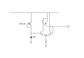
I'm really distracted right now. Here is a basic concept drawing. www.mouser.com lists over 28,000 op-amps. Feel free to try the other 27,999 variations of an op-amp in this drawing.
 

Attachments

crutschow

Joined Mar 14, 2008
38,912
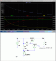
It's rather simple. The PNP is used as an emitter follower that drives the NPN emitter follower.
Since the two base emitter drops are of opposite polarity, they tend to cancel each other so the output has a low offset compared to the input.
The voltages don't completely cancel because the emitter currents are different for the two transistors.
The bias resistor R1 was selected based upon the simulations to give the lowest offset for the shown variation in load current.

You might try downloading the free LTspice program from Linear Technology and run the .asc file I posted of the circuit to experiment with it yourself.

Edit: Note that, as an added bonus, the PNP base-emitter voltage change due to ambient temperature will tend to be cancelled (balanced) by the NPN base-emitter change, so any output offset change with temperature from the transistors will be significantly lower than for a single transistor (the simulation shows about a factor of 7.5 reduction).
 
Last edited:

DickCappels

Joined Aug 21, 2008
10,661
You should be able to tune out some of that remaining 100 mv offset by adjusting one of the emitter resistors. At some point you might want to select pairs of transistors and thermally couple them. Or #12's suggestion, close the loop with an opamp.
 

crutschow

Joined Mar 14, 2008
38,912
I read about monolithic pairs in the 1970's. Now, you can buy them.
So happy about modern availability! :)
Since the two transistors are stated as being isolated in that particular example, I think they are two separate dies in the same package, and not monolithic on the same die.
 
Last edited:

#12

Joined Nov 30, 2010
18,224
Since the two transistors are stated as being isolated in that particular example, I think they are two separate dies in the same package, and not monolithic on the same die.
???
I believe you're correct on this part number, but I have also found monolithic matched differential pairs which were very convenient when I had to replace two horribly mis-matched, individually packaged transistors in a 200 watt audio amplifier.

Yeah, I know...put it back the way you found it, but I just couldn't resist. :)
That amplifier had 0.4 volts error, base to base, in the input pair. :eek:
 

crutschow

Joined Mar 14, 2008
38,912
I believe you're correct on this part number, but I have also found monolithic matched differential pairs which were very convenient when I had to replace two horribly mis-matched, individually packaged transistors in a 200 watt audio amplifier.
................
Yes, matched transistor pairs of the same polarity can be readily made on the same substrate, but it's not so easy to do for an NPN-PNP pair unless you use some form of dielectric isolation on the chip.
 
Top