 Facebook
 Google
 GitHub
 Linkedin
Hi all,
I am repairing a 200A welder. The circuit's main topology is full-bridge converter. For the schematic, please look at the pdf file. The welder has 3 PCBs.
The first board is just a DC rectifier (presented by the 326 Vdc on the first page).
The second board is the rest of the first page. It has an auxiliary flyback converter (AUX) to generate +24Vdc for the PWMIC (SG3525 and its peripheral components) and the gate driver. The gate driver drives the H-bridge (bottom-left of the 1st page).
The third board receives the output of the aforementioned H-bridge via its transformers and then rectifies it to DC output.
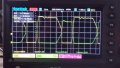
I want to test only board 2. So, I connect the circuit only in page 1. Coming back to the AUX flyback, I probed its MOSFET's Vds, and output diode's V(cathode) - V(anode). I can see some noises (jpg file "Wavenoise"). This noise also goes to +24V.
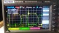
So, I cut the trace to separate the H-bridge from the primary ground (GNDPRI). The noise disappears! (jpg file "Waveok").
I rejoin the cut. What I have done so far to solve the issue:
1. Change the h-bridge snubber resistor from 47ohm to 18 ohm. --> The ringing amplitude is slightly less. Its duration is much lower
2. Change the h-bridge snubber capacitor from 470pF to 14.7 nF --> The snubber resistors were very hot. The ringing amplitude and duration are almost the same.
3. Change the 6.8 ohms gate drive to 10 ohms --> No significant changes of the amplitude. The duration of ringing is longer
4. Check the Vgs of each H-bridge mosfet. It was like below
 From all of my experiments, is it only this loop that cause the problem: B+ --- Cds --- GNDPRI --- its inductance?
Would the inductance of the gate drive transformer be a problem too?
If so, why I don't see any ringing when I cut the GNDPRI away from the H-bridge?
BlackMelon
I am repairing a 200A welder. The circuit's main topology is full-bridge converter. For the schematic, please look at the pdf file. The welder has 3 PCBs.
The first board is just a DC rectifier (presented by the 326 Vdc on the first page).
The second board is the rest of the first page. It has an auxiliary flyback converter (AUX) to generate +24Vdc for the PWMIC (SG3525 and its peripheral components) and the gate driver. The gate driver drives the H-bridge (bottom-left of the 1st page).
The third board receives the output of the aforementioned H-bridge via its transformers and then rectifies it to DC output.
I want to test only board 2. So, I connect the circuit only in page 1. Coming back to the AUX flyback, I probed its MOSFET's Vds, and output diode's V(cathode) - V(anode). I can see some noises (jpg file "Wavenoise"). This noise also goes to +24V.
So, I cut the trace to separate the H-bridge from the primary ground (GNDPRI). The noise disappears! (jpg file "Waveok").
I rejoin the cut. What I have done so far to solve the issue:
1. Change the h-bridge snubber resistor from 47ohm to 18 ohm. --> The ringing amplitude is slightly less. Its duration is much lower
2. Change the h-bridge snubber capacitor from 470pF to 14.7 nF --> The snubber resistors were very hot. The ringing amplitude and duration are almost the same.
3. Change the 6.8 ohms gate drive to 10 ohms --> No significant changes of the amplitude. The duration of ringing is longer
4. Check the Vgs of each H-bridge mosfet. It was like below
From all of my experiments, is it only this loop that cause the problem: B+ --- Cds --- GNDPRI --- its inductance?Would the inductance of the gate drive transformer be a problem too?
If so, why I don't see any ringing when I cut the GNDPRI away from the H-bridge?
BlackMelon
Attachments
-
 139.7 KB Views: 4
 -
 182.2 KB Views: 4
 -
985.7 KB Views: 5


