Facebook
 Google
 GitHub
 Linkedin
Hello!
I need to decide what I should understand/learn to go ahead with my boost converter and stop killing my MOSFETS in the wild.
I'm not a engineer (at least not one of the 'right type') and electronics is just a hobby.
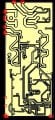
I have a boost converter that's basically scheme.jpg (MOSFETS are IRF640).
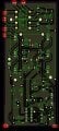
board.jpg is my testing board.
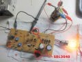
The flyback diodes are SBL3040 https://www.vishay.com/docs/88732/sbl3030p.pdf
I have PWM at fixed duty cycle and adjusted (hopefully) it's frequency for the best efficiency (higher possible output DC voltage with the fixed load) and it's around 16KHz
If I leave circuit running without the flyback diodes the MOSFETS gets hot (i cant touch them anymore) after 30 seconds.
If I leave it running with the flyback diodes the MOSFETS are almost just warm after 90 seconds but the robust SBL3040 pair gets hot (i cant touch them anymore).
scope1.jpg shows signal at MOSFET gate with the SBL3040 pair
scope2.jpg shows the same gate signal without the SBL3040 pair
Now I'm curious about:
Are the built-in MOSFETS diodes making them hot running the circuit without the external diodes?
What I need to go ahead investigating/learning to have this system equalized? Or maybe my approach to this is just wrong?
I often see in circuits of this type a capacitor and resistor connected in each of the primary coils. Possibly a filter but I dont know what are they doing or how to calculate them. Like in this example choppercaps.jpg
Perhaps that's what I need? Then again I cannot understand what they are doing.
Any tips/suggestion is appreciated!
Thanks!
I need to decide what I should understand/learn to go ahead with my boost converter and stop killing my MOSFETS in the wild.
I'm not a engineer (at least not one of the 'right type') and electronics is just a hobby.
I have a boost converter that's basically scheme.jpg (MOSFETS are IRF640).
board.jpg is my testing board.
The flyback diodes are SBL3040 https://www.vishay.com/docs/88732/sbl3030p.pdf
I have PWM at fixed duty cycle and adjusted (hopefully) it's frequency for the best efficiency (higher possible output DC voltage with the fixed load) and it's around 16KHz
If I leave circuit running without the flyback diodes the MOSFETS gets hot (i cant touch them anymore) after 30 seconds.
If I leave it running with the flyback diodes the MOSFETS are almost just warm after 90 seconds but the robust SBL3040 pair gets hot (i cant touch them anymore).
scope1.jpg shows signal at MOSFET gate with the SBL3040 pair
scope2.jpg shows the same gate signal without the SBL3040 pair
Now I'm curious about:
Are the built-in MOSFETS diodes making them hot running the circuit without the external diodes?
What I need to go ahead investigating/learning to have this system equalized? Or maybe my approach to this is just wrong?
I often see in circuits of this type a capacitor and resistor connected in each of the primary coils. Possibly a filter but I dont know what are they doing or how to calculate them. Like in this example choppercaps.jpg
Perhaps that's what I need? Then again I cannot understand what they are doing.
Any tips/suggestion is appreciated!
Thanks!
Attachments
-
 147.5 KB Views: 57
 -
 11.7 KB Views: 72
 -
 80 KB Views: 72
 -
 240.3 KB Views: 62
 -
 121.5 KB Views: 40
") . I will try to discover more about this one specific, if enough for the task as I cant decide this yet. Will try to get Schottky ones anyway.
. I will try to discover more about this one specific, if enough for the task as I cant decide this yet. Will try to get Schottky ones anyway.