Facebook
 Google
 GitHub
 Linkedin
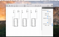
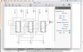
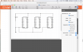
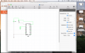
Today in my first electrical engineering lab we used the chips 7404, 7408, and 7432 to perform the equation
P(x,y,z) = x ˑ(y + z) + y’ˑz. We put the chips on to a breadboard which was connected to a C.A.D.E.T Testing system. (I just bought one for myself for some home practice, not sure how useful it will be but I want to make sure I have the resources I need to understand all of this stuff) But any way, I guess I should provide some background info on myself before I get into the problems I'm having. I am a freshman in college and this is my second week in the Electrical Engineering program at my school. I consider myself to be smart, but not crazy smart. The terminology I use is probably going to be off so I would love some feedback critiquing what I say. So far we have only covered the basics. Not, And, and Or Gates as well as corresponding truth tables and diagrams of Basic Boolean Algebraic equations. I get how to do all of this on paper but when it comes to implementing it on the breadboard, switches, and Led I'm a little bit lost. I was with a guy (my partner in lab) that had tons of experience wiring cars so he went through it without any issues however I didn't learn very much. I get how to connect the individual chips to power and ground but when implementing the equation onto the board I'm a little lost. I will be uploading pictures of the lab a little later if it would help you guys help me. Im not really sure how much information I should be telling you or if I'm missing something important. So anyway, all I'm asking is how to implement the variables (switches) to the three chips and how to carry out the equation between them to where the LED responds according to what the output of the equation should be. Thanks for your help and if you need any clarification on anything to help me out please ask and ill make sure to respond as fast as I can.
P(x,y,z) = x ˑ(y + z) + y’ˑz. We put the chips on to a breadboard which was connected to a C.A.D.E.T Testing system. (I just bought one for myself for some home practice, not sure how useful it will be but I want to make sure I have the resources I need to understand all of this stuff) But any way, I guess I should provide some background info on myself before I get into the problems I'm having. I am a freshman in college and this is my second week in the Electrical Engineering program at my school. I consider myself to be smart, but not crazy smart. The terminology I use is probably going to be off so I would love some feedback critiquing what I say. So far we have only covered the basics. Not, And, and Or Gates as well as corresponding truth tables and diagrams of Basic Boolean Algebraic equations. I get how to do all of this on paper but when it comes to implementing it on the breadboard, switches, and Led I'm a little bit lost. I was with a guy (my partner in lab) that had tons of experience wiring cars so he went through it without any issues however I didn't learn very much. I get how to connect the individual chips to power and ground but when implementing the equation onto the board I'm a little lost. I will be uploading pictures of the lab a little later if it would help you guys help me. Im not really sure how much information I should be telling you or if I'm missing something important. So anyway, all I'm asking is how to implement the variables (switches) to the three chips and how to carry out the equation between them to where the LED responds according to what the output of the equation should be. Thanks for your help and if you need any clarification on anything to help me out please ask and ill make sure to respond as fast as I can.