 Facebook
 Google
 GitHub
 Linkedin
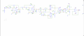
Hi everyone. I've designed a circuit for small amplitude signal processing (amplitude = 1 mV). As for active filtering stages I use 2nd order LPF (fc = 20Hz), 2nd order HPF (fc=4Hz) and twin-t notch filter (50Hz). After that goes amplification stage (op amp with potentiometer as a negative feedback), offset control and output buffer stage. As for power supplies, I use 3.7V battery and 7660 voltage converter for negative supply. I don't use decoupling on power rails (can it be the thing?)
I have a problem with amplification stage. When I try to increase the gain, I start to see slow oscillations (somewhere in between of 20-40Hz) instead of a signal.
How can I deal with those oscillations? Should I use a buffer between filtering and amplification stages?
I've already implemented a capacitor in parallel with negative feedback resistor, but It doesn't have the desired effect.
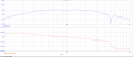
I've attached Bode plot and the circuit.
Thanks in advance!
I have a problem with amplification stage. When I try to increase the gain, I start to see slow oscillations (somewhere in between of 20-40Hz) instead of a signal.
How can I deal with those oscillations? Should I use a buffer between filtering and amplification stages?
I've already implemented a capacitor in parallel with negative feedback resistor, but It doesn't have the desired effect.
I've attached Bode plot and the circuit.
Thanks in advance!
Attachments
-
 275.5 KB Views: 25
 -
 346 KB Views: 24


