 Facebook
 Google
 GitHub
 Linkedin
Hi, I'm posting a thread due to a problem while designing type III compensator for a boost converter.
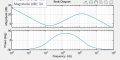
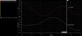
According to condition for compensator output voltage (Vc) to power stage output voltage (VOUT) which are consisting modulator under 1MHz switching frequency, I decided compensator's component parameters. The result for compensator's transfer function's frequency response is attatched. Target crossover frequency of loop gain is 150kHz, and phase margin is 60 degree.
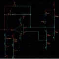
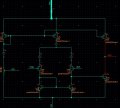
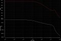
In, cadence, I designed an op amp for amplifier part of the compensator and run ac simulation. However, the actual plot has additonal phase shift beyond switching frequency. I'm expecting it is due to RHP zero of the op amp, but have no idea of how to fix or redesign the op amp part for the compensator.
What I want to know is "how to decide the op amp's spec (bandwidth, GBW)" under given switching frequency and targetted crossover frequency. I have searched some documents about op-amp's non ideal characteristic.
Would be huge appreciation if I can get some idea or fundamentals of how to design op amp for type-III compensator.
According to condition for compensator output voltage (Vc) to power stage output voltage (VOUT) which are consisting modulator under 1MHz switching frequency, I decided compensator's component parameters. The result for compensator's transfer function's frequency response is attatched. Target crossover frequency of loop gain is 150kHz, and phase margin is 60 degree.
In, cadence, I designed an op amp for amplifier part of the compensator and run ac simulation. However, the actual plot has additonal phase shift beyond switching frequency. I'm expecting it is due to RHP zero of the op amp, but have no idea of how to fix or redesign the op amp part for the compensator.
What I want to know is "how to decide the op amp's spec (bandwidth, GBW)" under given switching frequency and targetted crossover frequency. I have searched some documents about op-amp's non ideal characteristic.
Would be huge appreciation if I can get some idea or fundamentals of how to design op amp for type-III compensator.
Attachments
-
 33.1 KB Views: 9
 -
 75.6 KB Views: 11
 -
 87 KB Views: 11
 -
 100.7 KB Views: 11
 -
 131.7 KB Views: 10


