DIY Geiger Counter – Looking for Feedback on the Schematic and PCB Design

Thread Starter

SmektHet

Joined Aug 12, 2026
5
1786544687818.png
1786544699718.pngHi everyone,

I'm working on a high-voltage circuit and I'd like to get some advice before I order the PCB.

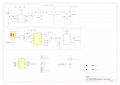
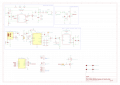
The circuit generates around 400 V at low current. The HV section uses a TLC555-based oscillator, an inductor and a switching transistor to step the voltage up from 5 V to around 400 V. There's also a separate impulse detection section.

The lower part of the schematic is the USB-C/battery charging and 5 V power supply.

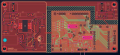
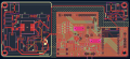
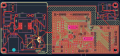
I've attached both my current schematic and PCB layout.

The stack-up is as follows:
  • Signals
  • Ground <- only for LV section
  • Signals / Power
  • Ground <- only for LV section
I'm mainly looking for some advice on the PCB layout:

  1. 1. What's the best way to handle the ground in the HV section? Should I use a copper pour or individual traces?
  2. 2. How much clearance should I leave between the 400 V traces and GND copper?
  3. 3. Are there any particular components or nodes in the schematic that I should give extra spacing around?
  4. 4. Is there anything obviously wrong with having the HV section and the USB/battery circuitry on the same PCB?
  5. 5. Would an isolation slot or something similar be recommended anywhere?

I'd also appreciate any feedback on the schematic itself.

Thanks!
 
Which tube are you using?
PCB trace spacing for 400VDC is 2.0mm for Pollution Degree 2 (this is not to be confused with mains clearances as they include extra room for overvoltage transients of many kV). It depends on dust, dirt, humidity but 1.0mm is the minimum I would guess.

I have time later to markup the sensitive schematic traces.
 

Thread Starter

SmektHet

Joined Aug 12, 2026
5
Which tube are you using?
PCB trace spacing for 400VDC is 2.0mm for Pollution Degree 2 (this is not to be confused with mains clearances as they include extra room for overvoltage transients of many kV). It depends on dust, dirt, humidity but 1.0mm is the minimum I would guess.

I have time later to markup the sensitive schematic traces.
I am using the SBM-20

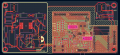
here is also a updated image of my PCB:
I changed the ground plane to traces, as someone said to me that this was a better method.
1786649434391.png
 
For the PCB layout, it looks OK except for the (high current) GND trace from Q2-E to the battery/power. It's too long a snakey run. I would use thicker traces for it.
Spacings look OK except between CR1's pads, more on that later.
C2 polarity marking looks backwards unless it's a polymer cap. How about a + mark.
SW2 the wiper pin2 must be connected.
C6 is a little small for value, I would count on ending up using a bigger part like 100nF as you won't get 47nF at voltage with ceramic caps. I'm saying your 47nF cap is much less than that at 400V.
ESP32 don't have a ground-pour right under the chip antenna. Espressif/antenna manufacturer give a spec for clearance, maybe check it unless you are using the external antenna version.
edit: TVS D1 what is that about? USB C shield to GND doesn't need a 5V TVS. Did you mean to have it on on VBUS?

OK I see the schematic is largely copypasta possibly starting before from OpenRad or some other blogger. I would say the circuit design has some issues.
Mainly the Impulse Detector C11 at 220pF is too big and would lower sensitivity. I wonder why it's there even, somebody must have had a noise problem or lousy F/W to pulse stretch. I would leave the footprint but not populate it, see how things work without it. Finding the Townsend discharge spec for a SBM-20 not easy, datasheets are in Cyrillic. My point is a few pulses most likely too small to do much to charge 220pF cap, many pulses are needed to make what looks like one pulse, and so it's not an accurate Geiger counter.

CR1 is a "standard recovery" diode and a bit slow at 1.8usec recovery, SMF package, 1,000PIV 0.7A I would consider SMA package. Even a 600V part is enough. FR1J is 600V 0.25usec recovery, US1M looks best.

Q2 is huge TO-220 considering current-limit is 47mA at Q1. Is R3 right at 15 ohms? And Q2 has low beta typical for HV transistors.
 
Last edited:

Thread Starter

SmektHet

Joined Aug 12, 2026
5
Thanks for the time that you have spend to look over my PCB. As you may have already noticed this is my first time making a PCB, so i do appreciate all the time you spend to help me.

"C2 polarity marking looks backwards unless it's a polymer cap. How about a + mark."
I was planning on using a CAP ALUM 100UF 20% 35V RADIAL TH. Now that you say it the + mark is hidden under the gnd wire and you are right its backwards.

"SW2 the wiper pin2 must be connected."
Ah yes I see the mistake.

"C6 is a little small for value, I would count on ending up using a bigger part like 100nF as you won't get 47nF at voltage with ceramic caps. I'm saying your 47nF cap is much less than that at 400V."
Could i also use the B32642H6473J000 since its a PP it should hold better at high voltages right?

"ESP32 don't have a ground-pour right under the chip antenna. Espressif/antenna manufacturer give a spec for clearance, maybe check it unless you are using the external antenna version."
This is not a official ESP board so it's hard to find the exact clearance, but added a 10mm clearance. I know there are not supposed to be traces or other stuff in the zone but otherwise I need to remake my whole PCB and this is just version 1. I want to test the High voltage first before adding more stuff on the board.


"TVS D1 what is that about? USB C shield to GND doesn't need a 5V TVS. Did you mean to have it on on VBUS?"
Yes this was supposed to be on the VBUS.


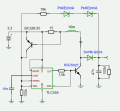
The source for my geigercounter circuit is: https://www.mikrocontroller.net/topic/380666 with the following circuit:
So that's also why i put the 15 Ohm for R3.
1786714805445.png

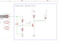
and i used the following circuit for the pulse counting:
1786715744752.png
from mightyohm.com

I will try it without C11 to see how it works, according to LTspice it should also work without.

"CR1 is a "standard recovery" diode and a bit slow at 1.8usec recovery, SMF package, 1,000PIV 0.7A I would consider SMA package. Even a 600V part is enough. FR1J is 600V 0.25usec recovery, US1M looks best."
Yes, I see your point. I changed it to a US1M with 1000v 75 ns recovery.

"Q2 is huge TO-220 considering current-limit is 47mA at Q1. Is R3 right at 15 ohms? And Q2 has low beta typical for HV transistors."
I changed it to a KSC5026MOS, its smaller and it needs less mA.


Updated schematic and PCB:
1786728405648.png1786729424507.png
 
The ESP32C3 antenna clearance is near the antenna, not the entire PCB section (hatched line) perimeter.
So I would say the ground fill near your "U2" text needs to be redone, looks like it's blocking it.
Pic taken from https://docs.espressif.com/projects...ines/en/latest/esp32c3/pcb-layout-design.html
There are Aliex C3 modules with a bad (chip) antenna design out there, if you search for that you can see what they look like and avoid buying them.

It's hard for me to give a thumbs up on minimalist circuits that float around the Internet and get a change or two, copied etc. Then some people are on several forums getting advice and things keep changing.
I've never gotten 400V right off the bat, it's typically a 3-stage voltage multiplier but I have not poked around with a scope to see how this version does. This is my way to evaluate a circuit, then I give it the rubber stamp.

The boost converter high current paths - first DC power is a long skinny trace C3 to the ESP32 5V pin... I would fatten the trace, and the Q2-E ground path, jump over to the pour at C3 or C2.

I don't see thermal reliefs used, which will make soldering difficult for J3-2, J4-1, SW2-2, DC-USB switch, Q3-E etc. It will take lots of heat to solder those and might be impossible.
R25, R23, R22 can be small SMT parts not big though-hole parts.
The ESP32-C3 can you use the USB connector with stuff in front of it like Q4 and the tube clip F2? To program it. Or you plan to pull it off, if it's on header sockets?
 

Thread Starter

SmektHet

Joined Aug 12, 2026
5
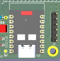
Sorry for not clarifying but the USB-connector is at the bottom and the antenna is at the top. So accessing the USB is no problem. And that is also why I put the NO ground zone there. I also checked my ESP32C3 and it looks like that I have the correct ones, according to the distance of the clearance.
1786974058632.png

The hatched line perimeter is for adding a distance between HV and LV. (just to be safe)

For R22, R23 and R25 I don't really know how much voltage will be on them so that's why i chose the through-hole parts at first. But I changed them now to SMD components. And I also changed back to thermal reliefs, instead of solid. I thought the solid is better for SMD components? But I do get what you are saying with soldering difficulty of all the through-hole components if its solid.
1786974208682.png
 
High voltage is at the other end of the tube, so the impulse detector can be SMT parts. Small blips there.
If you need pulse stretching (for the firmware) I would leave provision for a small cap across Q4 E-C or C-GND (not use C11 for that).
I have not seen the software to see how they are counting pulses.
ESP32 unfortunately does not have input/output capture general purpose timers, so you have to use an interrupt in the middle of a bunch of other interrupt (priorities).

Problem with using no PCB thermal reliefs is any soldering must heat up the entire pour as well. It takes too much heat for an iron. Using no thermal reliefs is where you need to conduct heat away for cooling and are using reflow/hot plate etc.

The ESP32 TX chirp can be fairly strong so PCB traces close to the antenna might pick up some of that? But here they are for the display and no idea if Q4 could pick some of that up. I haven't checked how much interference there could be, but not a problem in my stuff so far. It's a risk. I would just get a prototype board made and see how it does.
 
Since this is the first version, I agree that making a prototype and testing it is probably the best next step.

One small point from the SMT equipment side: if you plan to order assembled boards, check the pick-and-place file preview carefully before submitting it. I would pay particular attention to the rotation and origin of the ESP32 module, diodes and other polarized parts. These are common places for the CAD footprint and the assembly data to disagree.

Changing the ground connections back to thermal reliefs also makes sense, especially if you may need to replace or rework parts during testing. For a hand-assembled prototype, I would not worry too much about panel rails or fiducials yet. The assembler can advise on those if you later order a larger quantity.
 

Thread Starter

SmektHet

Joined Aug 12, 2026
5
Since this is the first version, I agree that making a prototype and testing it is probably the best next step.

One small point from the SMT equipment side: if you plan to order assembled boards, check the pick-and-place file preview carefully before submitting it. I would pay particular attention to the rotation and origin of the ESP32 module, diodes and other polarized parts. These are common places for the CAD footprint and the assembly data to disagree.

Changing the ground connections back to thermal reliefs also makes sense, especially if you may need to replace or rework parts during testing. For a hand-assembled prototype, I would not worry too much about panel rails or fiducials yet. The assembler can advise on those if you later order a larger quantity.
I will be soldering it myself. This is my first ever PCB but I do have plenty of experience with soldering through-hole and SMD components.
 
Top