DIY Geiger Counter – Looking for Feedback on the Schematic and PCB Design

Thread Starter

SmektHet

Joined Aug 12, 2026
2
1786544687818.png
1786544699718.pngHi everyone,

I'm working on a high-voltage circuit and I'd like to get some advice before I order the PCB.

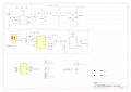
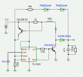
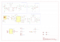
The circuit generates around 400 V at low current. The HV section uses a TLC555-based oscillator, an inductor and a switching transistor to step the voltage up from 5 V to around 400 V. There's also a separate impulse detection section.

The lower part of the schematic is the USB-C/battery charging and 5 V power supply.

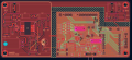
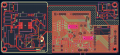
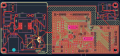
I've attached both my current schematic and PCB layout.

The stack-up is as follows:
  • Signals
  • Ground <- only for LV section
  • Signals / Power
  • Ground <- only for LV section
I'm mainly looking for some advice on the PCB layout:

  1. 1. What's the best way to handle the ground in the HV section? Should I use a copper pour or individual traces?
  2. 2. How much clearance should I leave between the 400 V traces and GND copper?
  3. 3. Are there any particular components or nodes in the schematic that I should give extra spacing around?
  4. 4. Is there anything obviously wrong with having the HV section and the USB/battery circuitry on the same PCB?
  5. 5. Would an isolation slot or something similar be recommended anywhere?

I'd also appreciate any feedback on the schematic itself.

Thanks!
 
Which tube are you using?
PCB trace spacing for 400VDC is 2.0mm for Pollution Degree 2 (this is not to be confused with mains clearances as they include extra room for overvoltage transients of many kV). It depends on dust, dirt, humidity but 1.0mm is the minimum I would guess.

I have time later to markup the sensitive schematic traces.
 

Thread Starter

SmektHet

Joined Aug 12, 2026
2
Which tube are you using?
PCB trace spacing for 400VDC is 2.0mm for Pollution Degree 2 (this is not to be confused with mains clearances as they include extra room for overvoltage transients of many kV). It depends on dust, dirt, humidity but 1.0mm is the minimum I would guess.

I have time later to markup the sensitive schematic traces.
I am using the SBM-20

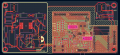
here is also a updated image of my PCB:
I changed the ground plane to traces, as someone said to me that this was a better method.
1786649434391.png
 
For the PCB layout, it looks OK except for the (high current) GND trace from Q2-E to the battery/power. It's too long a snakey run. I would use thicker traces for it.
Spacings look OK except between CR1's pads, more on that later.
C2 polarity marking looks backwards unless it's a polymer cap. How about a + mark.
SW2 the wiper pin2 must be connected.
C6 is a little small for value, I would count on ending up using a bigger part like 100nF as you won't get 47nF at voltage with ceramic caps. I'm saying your 47nF cap is much less than that at 400V.
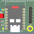
ESP32 don't have a ground-pour right under the chip antenna. Espressif/antenna manufacturer give a spec for clearance, maybe check it unless you are using the external antenna version.
edit: TVS D1 what is that about? USB C shield to GND doesn't need a 5V TVS. Did you mean to have it on on VBUS?

OK I see the schematic is largely copypasta possibly starting before from OpenRad or some other blogger. I would say the circuit design has some issues.
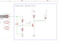
Mainly the Impulse Detector C11 at 220pF is too big and would lower sensitivity. I wonder why it's there even, somebody must have had a noise problem or lousy F/W to pulse stretch. I would leave the footprint but not populate it, see how things work without it. Finding the Townsend discharge spec for a SBM-20 not easy, datasheets are in Cyrillic. My point is a few pulses most likely too small to do much to charge 220pF cap, many pulses are needed to make what looks like one pulse, and so it's not an accurate Geiger counter.

CR1 is a "standard recovery" diode and a bit slow at 1.8usec recovery, SMF package, 1,000PIV 0.7A I would consider SMA package. Even a 600V part is enough. FR1J is 600V 0.25usec recovery, US1M looks best.

Q2 is huge TO-220 considering current-limit is 47mA at Q1. Is R3 right at 15 ohms? And Q2 has low beta typical for HV transistors.
 
Last edited:
Top